Understanding PCB tolerance
PCB tolerance is a critical aspect of PCB design and manufacturing. It defines the acceptable range of deviation from the ideal or specified dimensions and measurements. These tolerances are necessary to ensure that the PCB fits properly within the designated space in the electronic device, connects correctly with other components, and functions as intended.
Types of PCB Tolerances
There are several types of tolerances that need to be considered when designing and manufacturing PCBs:
- Dimensional Tolerance
- Hole Size Tolerance
- Copper Thickness Tolerance
- Solder Mask Tolerance
- Silkscreen Tolerance
- Electrical Tolerance
Dimensional Tolerance
Dimensional tolerance refers to the acceptable variation in the physical dimensions of the PCB, such as length, width, and thickness. The dimensional tolerance is typically specified in millimeters (mm) or inches (in) and varies depending on the size and complexity of the PCB.
| PCB Dimension | Typical Tolerance |
|---|---|
| Length | ±0.2 mm |
| Width | ±0.2 mm |
| Thickness | ±10% |
It is essential to maintain tight dimensional tolerances to ensure proper fit and compatibility with other components in the electronic device.
Hole Size Tolerance
Hole size tolerance refers to the acceptable variation in the diameter of the drilled holes on the PCB. These holes are used for mounting components, such as through-hole devices, and for creating vias that connect different layers of the PCB.
| Hole Diameter | Typical Tolerance |
|---|---|
| 0.3 mm | ±0.05 mm |
| 0.5 mm | ±0.05 mm |
| 1.0 mm | ±0.1 mm |
Maintaining accurate hole size tolerances is crucial for ensuring proper component fit and reliable electrical connections.
Copper Thickness Tolerance
Copper thickness tolerance refers to the acceptable variation in the thickness of the copper traces on the PCB. The copper thickness is typically measured in ounces per square foot (oz/ft²) or microns (µm).
| Copper Thickness | Typical Tolerance |
|---|---|
| 1 oz/ft² | ±20% |
| 2 oz/ft² | ±10% |
| 3 oz/ft² | ±10% |
Accurate control of copper thickness is essential for maintaining the desired electrical properties and current-carrying capacity of the PCB Traces.
Solder Mask Tolerance
Solder mask tolerance refers to the acceptable variation in the registration and alignment of the solder mask layer on the PCB. The solder mask is a protective coating applied to the PCB to prevent accidental short circuits and protect the copper traces from oxidation.
| Solder Mask Parameter | Typical Tolerance |
|---|---|
| Registration | ±0.05 mm |
| Alignment | ±0.05 mm |
Precise solder mask tolerances are necessary to ensure proper insulation and protection of the PCB traces and pads.
Silkscreen Tolerance
Silkscreen tolerance refers to the acceptable variation in the registration and alignment of the silkscreen layer on the PCB. The silkscreen is used to print text, logos, and component outlines on the PCB for easy identification and assembly.
| Silkscreen Parameter | Typical Tolerance |
|---|---|
| Registration | ±0.1 mm |
| Alignment | ±0.1 mm |
Accurate silkscreen tolerances are important for clear and legible markings on the PCB.
Electrical Tolerance
Electrical tolerance refers to the acceptable variation in the electrical properties of the PCB, such as resistance, capacitance, and inductance. These tolerances are dependent on the materials used, the design of the PCB, and the manufacturing process.
| Electrical Parameter | Typical Tolerance |
|---|---|
| Resistance | ±10% |
| Capacitance | ±10% |
| Inductance | ±10% |
Maintaining electrical tolerances within acceptable ranges is crucial for ensuring the proper functioning and performance of the electronic device.
Factors Affecting PCB Tolerance
Several factors can influence the achievable tolerances in PCB manufacturing:
- Manufacturing Process
- Material Selection
- PCB Complexity
- Environmental Conditions
Manufacturing Process
The manufacturing process used to produce the PCB can significantly impact the achievable tolerances. Different manufacturing techniques, such as etching, drilling, and plating, have their own inherent limitations and variability.
For example, the etching process used to create the copper traces on the PCB can introduce variations in the width and thickness of the traces. Similarly, the drilling process used to create holes in the PCB can introduce variations in the hole diameter and position.
To minimize the impact of manufacturing process variations, it is essential to work closely with the PCB Manufacturer and understand their capabilities and limitations. Selecting a reputable manufacturer with a proven track record of producing high-quality PCBs can help ensure tighter tolerances and more consistent results.
Material Selection
The choice of materials used in the PCB manufacturing process can also impact the achievable tolerances. Different PCB substrates, such as FR-4, Rogers, or polyimide, have different mechanical and electrical properties that can affect the dimensional stability and performance of the PCB.
For example, FR-4 is a commonly used PCB substrate material known for its good mechanical strength and electrical insulation properties. However, it is also prone to dimensional changes due to moisture absorption and thermal expansion. On the other hand, polyimide substrates offer better dimensional stability and Thermal Resistance but are more expensive.
Careful selection of PCB materials based on the specific requirements of the application can help minimize the impact of material variations on the achievable tolerances.
PCB Complexity
The complexity of the PCB design can also influence the achievable tolerances. More complex PCBs with higher component density, smaller feature sizes, and tighter spacing requirements will typically have more stringent tolerance requirements compared to simpler designs.
For example, a high-density PCB with fine-pitch components and narrow trace widths will require tighter tolerances in terms of hole size, copper thickness, and solder mask registration compared to a more spacious design with larger components and wider traces.
To accommodate the increased complexity and tighter tolerance requirements, it may be necessary to use advanced manufacturing techniques, such as high-precision laser drilling or fine-line etching. Additionally, closer collaboration between the PCB designer and the manufacturer can help identify and address potential tolerance issues early in the design process.
Environmental Conditions
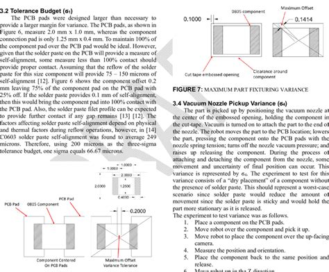
Environmental conditions, such as temperature, humidity, and vibration, can also impact the achievable tolerances in PCB manufacturing. Exposure to extreme temperatures or humidity can cause the PCB substrate to expand or contract, leading to dimensional changes and potential misalignment of components.
Similarly, vibration during the manufacturing process or in the end-use application can cause mechanical stress on the PCB, leading to potential damage or degradation of the electrical connections.
To mitigate the impact of environmental conditions on PCB tolerances, it is important to consider the expected operating conditions during the design phase and select materials and manufacturing processes that can withstand those conditions. Additionally, proper handling and storage of PCBs during manufacturing and assembly can help minimize exposure to adverse environmental factors.
Achieving Tight PCB Tolerances
Achieving tight PCB tolerances requires a combination of careful design, material selection, and close collaboration with the PCB manufacturer. Here are some key considerations for achieving tight tolerances:
- Design for Manufacturability (DFM)
- Communication with PCB Manufacturer
- Quality Control and Inspection
Design for Manufacturability (DFM)
Design for Manufacturability (DFM) is a design approach that takes into account the limitations and capabilities of the manufacturing process during the PCB design phase. By considering the manufacturing constraints early in the design process, designers can create PCBs that are easier to manufacture and more likely to meet the desired tolerances.
Some key DFM considerations for achieving tight tolerances include:
- Selecting appropriate trace widths and spacing based on the manufacturing capabilities
- Choosing component sizes and pitches that are compatible with the manufacturing process
- Avoiding unnecessary complexity in the PCB layout and routing
- Providing adequate clearances and tolerances for critical features
By following DFM guidelines and working closely with the PCB manufacturer, designers can optimize their designs for manufacturability and achieve tighter tolerances.
Communication with PCB Manufacturer
Effective communication with the PCB manufacturer is essential for achieving tight tolerances. Designers should provide clear and detailed specifications for the PCB, including the desired tolerances for critical dimensions and features.
It is also important to discuss the manufacturing capabilities and limitations with the manufacturer to ensure that the design is feasible and can be produced within the desired tolerances. The manufacturer can provide valuable feedback and suggestions for optimizing the design for manufacturability.
Regular communication and collaboration between the designer and the manufacturer throughout the manufacturing process can help identify and resolve any potential issues related to tolerances and ensure a successful outcome.
Quality Control and Inspection
Implementing robust quality control and inspection procedures is crucial for ensuring that the manufactured PCBs meet the desired tolerances. This involves several steps:
-
Incoming material inspection: Verifying that the raw materials used in the PCB manufacturing process meet the specified requirements and tolerances.
-
In-process inspection: Monitoring the PCB manufacturing process at various stages to ensure that the tolerances are being maintained and any deviations are identified and corrected promptly.
-
Final inspection: Conducting thorough visual and automated inspections of the finished PCBs to verify that all dimensions, features, and tolerances are within the acceptable range.
-
Electrical testing: Performing electrical tests to ensure that the PCB meets the specified electrical tolerances and functions as intended.
By implementing comprehensive quality control and inspection procedures, manufacturers can identify and address any tolerance issues early in the process, reducing the risk of defects and ensuring the delivery of high-quality PCBs that meet the desired specifications.

Frequently Asked Questions (FAQ)
-
What is PCB tolerance, and why is it important?
PCB tolerance refers to the acceptable range of variation in dimensions, measurements, and other parameters that can occur during the PCB manufacturing process without compromising the functionality and reliability of the final product. It is important because it ensures proper fit, compatibility, and performance of the PCB in the electronic device. -
What are the different types of PCB tolerances?
The different types of PCB tolerances include dimensional tolerance, hole size tolerance, copper thickness tolerance, solder mask tolerance, silkscreen tolerance, and electrical tolerance. Each type of tolerance addresses a specific aspect of the PCB manufacturing process and is critical for ensuring the overall quality and functionality of the PCB. -
How can I achieve tight PCB tolerances in my designs?
To achieve tight PCB tolerances, you should follow Design for Manufacturability (DFM) guidelines, select appropriate materials, and work closely with your PCB manufacturer. Communicate your tolerance requirements clearly, and consider the manufacturing capabilities and limitations when designing your PCB. Additionally, implementing robust quality control and inspection procedures can help ensure that the manufactured PCBs meet the desired tolerances. -
What factors can affect the achievable PCB tolerances?
Several factors can affect the achievable PCB tolerances, including the manufacturing process, material selection, PCB complexity, and environmental conditions. The manufacturing process and techniques used can introduce variations, while the choice of materials can impact the dimensional stability and performance of the PCB. More complex PCB designs with tighter spacing and smaller features will have more stringent tolerance requirements. Environmental conditions, such as temperature and humidity, can also cause dimensional changes and affect the tolerances. -
How can I ensure that my PCB meets the specified tolerances?
To ensure that your PCB meets the specified tolerances, work closely with your PCB manufacturer and communicate your requirements clearly. Provide detailed specifications and discuss the feasibility of achieving the desired tolerances based on the manufacturer’s capabilities. Implement comprehensive quality control and inspection procedures, including incoming material inspection, in-process monitoring, final inspection, and electrical testing. By taking these steps, you can identify and address any tolerance issues early in the process and ensure the delivery of high-quality PCBs that meet your specifications.
Conclusion
PCB tolerance is a critical aspect of PCB design and manufacturing, as it ensures the proper fit, compatibility, and performance of the PCB in the electronic device. Understanding the different types of tolerances, such as dimensional, hole size, copper thickness, solder mask, silkscreen, and electrical tolerances, is essential for designing and manufacturing high-quality PCBs.
Several factors can influence the achievable tolerances, including the manufacturing process, material selection, PCB complexity, and environmental conditions. To achieve tight tolerances, designers should follow Design for Manufacturability (DFM) guidelines, communicate effectively with the PCB manufacturer, and implement robust quality control and inspection procedures.
By carefully considering the tolerance requirements during the design phase, working closely with the PCB manufacturer, and ensuring thorough quality control, designers and manufacturers can produce PCBs that meet the desired specifications and perform reliably in the intended application.
Leave a Reply