In the ever-evolving world of electronics, High-Density Interconnect (HDI) PCBs have emerged as a game-changer for compact and high-performance electronic devices. As the demand for miniaturization and increased functionality continues to rise, HDI PCBs offer a viable solution to accommodate more components and interconnections within a smaller footprint. This comprehensive guide aims to provide a practical approach to HDI PCB layout and design, enabling engineers and designers to unlock the full potential of this advanced technology.
Fundamentals of HDI PCBs
Before delving into the intricacies of HDI PCB layout and design, it is essential to understand the fundamental concepts and characteristics of HDI PCBs.
1. HDI PCB Definition and Applications
HDI PCBs are characterized by their ability to accommodate a high density of interconnections and components within a compact space. These boards typically feature smaller feature sizes, such as finer trace widths, tighter spacing between traces, and higher via densities. HDI PCBs are widely used in various applications, including:
- Smartphones and tablets
- Wearable devices
- Medical equipment
- Aerospace and defense systems
- High-performance computing
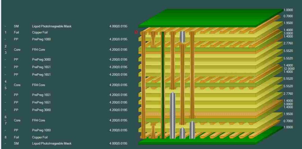
2. HDI PCB Construction and Materials
HDI PCBs are constructed using specialized materials and techniques to achieve their high-density capabilities. Some common materials used in HDI PCB construction include:
- Low-loss, high-frequency laminate materials (e.g., Rogers, Taconic)
- Resin-coated copper (RCC) foils or modified semi-additive process (MSAP) for fine-line circuitry
- High-performance dielectric materials with low dielectric constant and low dissipation factor
3. Key Advantages of HDI PCBs
HDI PCBs offer several advantages over conventional PCBs, including:
- Increased component density and miniaturization
- Improved signal integrity and high-frequency performance
- Reduced layer count and overall board thickness
- Enhanced thermal management capabilities
- Potential for cost savings and improved reliability
HDI PCB Layout and Design Guidelines
Designing HDI PCBs requires a thorough understanding of various layout considerations and design guidelines to ensure optimal performance and reliability.
1. Design Rules and Constraints
HDI PCB design involves adhering to strict design rules and constraints to accommodate the high-density interconnections. These rules typically include:
| Design Rule | Typical Range |
|---|---|
| Trace Width | 2-4 mils (50-100 μm) |
| Trace Spacing | 3-5 mils (75-125 μm) |
| Via Diameter | 6-8 mils (150-200 μm) |
| Via-to-Via Spacing | 8-10 mils (200-250 μm) |
| Pad Size | 10-12 mils (250-300 μm) |
It’s important to note that these values may vary depending on the specific HDI PCB technology and manufacturer capabilities.
2. Signal Integrity Considerations
Signal integrity is of paramount importance in HDI PCB design due to the high-density routing and high-frequency operation. Key considerations include:
- Controlled impedance routing
- Minimizing reflections and crosstalk
- Proper termination and decoupling
- Careful management of return paths and reference planes
3. Power Integrity and Thermal Management
HDI PCBs often feature high-power components and densely packed circuitry, leading to thermal management challenges. Proper power integrity and thermal management techniques must be employed, such as:
- Efficient power distribution networks
- Adequate decoupling and bypass capacitors
- Thermal vias and heat sinks for hot spots
- Thermal modeling and analysis
4. Component Placement and Routing
Efficient component placement and routing strategies are crucial for optimizing HDI PCB performance and manufacturability. Key considerations include:
- Minimizing trace lengths for critical signals
- Avoiding unnecessary bends and vias
- Proper fanout and routing for high-speed signals
- Maintaining clearance and spacing requirements
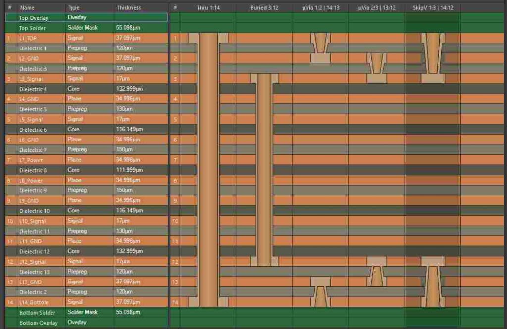
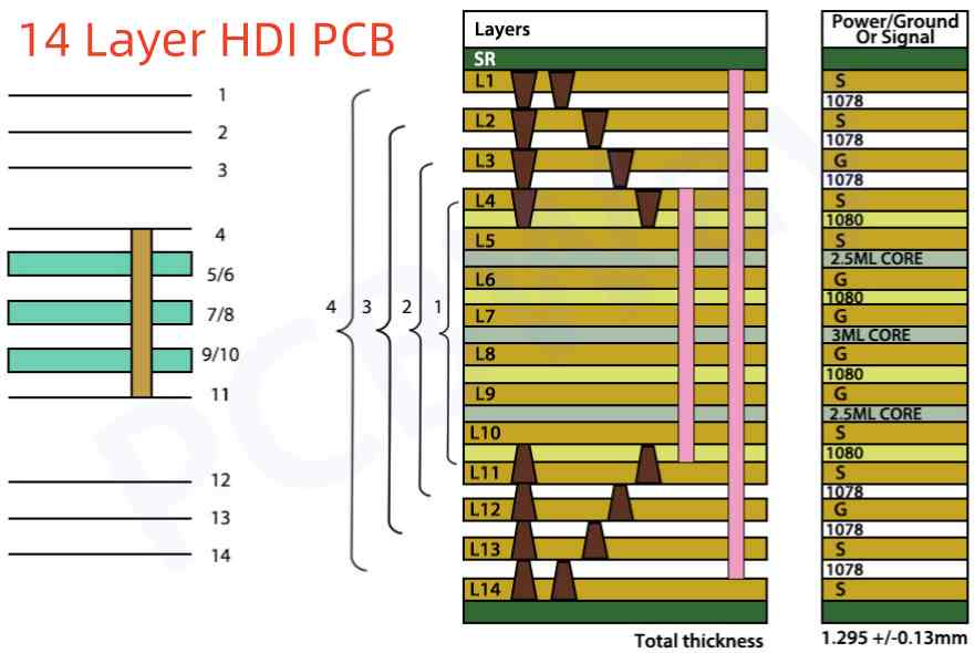
5. Manufacturing Considerations
HDI PCB manufacturing processes involve specialized techniques and stringent tolerances. Design considerations should account for:
- Laser-drilled microvias and buried vias
- Blind and buried via fabrication techniques
- Registration and alignment tolerances
- Surface finishes and solderable finishes
6. Design for Testability and Reliability
HDI PCBs often require specialized testing and validation methods due to their high complexity and density. Design considerations should include:
- Incorporating test points and access for in-circuit testing
- Designing for boundary scan and built-in self-test (BIST)
- Adherence to design for manufacturability (DFM) and design for reliability (DFR) guidelines
7. Design Verification and Simulation
Before proceeding to manufacturing, it is essential to thoroughly verify and simulate the HDI PCB design using appropriate software tools. Electromagnetic (EM) simulation, signal integrity analysis, and power integrity analysis can identify potential issues and optimize the design for optimal performance.
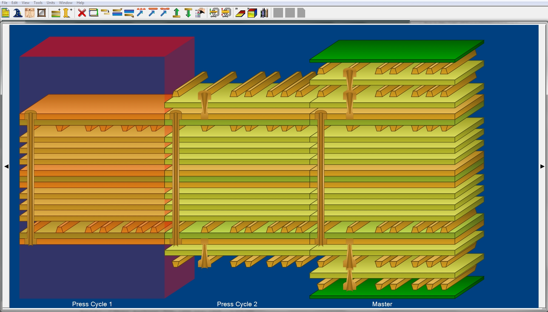
HDI PCB Design Flow
The HDI PCB design process typically follows a structured flow to ensure efficient and effective design implementation. The general design flow includes the following steps:
- Design Requirements and Specifications
- Schematic Capture and Component Selection
- HDI PCB Layout and Routing
- Design Rule Checking (DRC) and Constraint Validation
- Signal Integrity and Power Integrity Analysis
- Thermal Analysis and Optimization
- Design Verification and Simulation
- Manufacturing Preparation and Documentation
- Prototyping and Testing
- Design Iteration and Refinement
Throughout the design flow, close collaboration with HDI PCB manufacturers and adherence to best practices are essential for achieving successful HDI PCB designs.
Frequently Asked Questions (FAQ)
- What are the key differences between HDI PCBs and conventional PCBs? HDI PCBs are characterized by their ability to accommodate a higher density of interconnections and components within a smaller footprint. They typically feature finer trace widths, tighter spacing, and higher via densities compared to conventional PCBs. HDI PCBs also require specialized materials, manufacturing processes, and design considerations to ensure optimal performance and reliability.
- What are the main advantages of using HDI PCBs? The main advantages of HDI PCBs include increased component density and miniaturization, improved signal integrity and high-frequency performance, reduced layer count and overall board thickness, enhanced thermal management capabilities, and potential cost savings and improved reliability compared to conventional PCBs.
- What are some common materials used in HDI PCB construction? Common materials used in HDI PCB construction include low-loss, high-frequency laminate materials (e.g., Rogers, Taconic), resin-coated copper (RCC) foils or modified semi-additive process (MSAP) for fine-line circuitry, and high-performance dielectric materials with low dielectric constant and low dissipation factor.
- What are some critical design considerations for HDI PCBs? Critical design considerations for HDI PCBs include adhering to strict design rules and constraints, ensuring signal integrity and controlled impedance routing, proper power integrity and thermal management, efficient component placement and routing strategies, manufacturing considerations (e.g., laser-drilled microvias, buried vias), and designing for testability and reliability.
- What are some common challenges associated with HDI PCB design? Common challenges associated with HDI PCB design include managing high-density interconnections and component placement, ensuring signal integrity and mitigating crosstalk, addressing thermal management issues, adhering to stringent manufacturing tolerances, and designing for testability and reliability. Additionally, HDI PCB design often requires specialized design tools, simulation capabilities, and close collaboration with manufacturers.
By following the guidelines and best practices outlined in this comprehensive guide, engineers and designers can navigate the complexities of HDI PCB layout and design, enabling the development of compact, high-performance, and reliable electronic devices for a wide range of applications.


Leave a Reply