RayMing brings you reliable HDI printed circuit boards by ensuring meticulous planning in your stack-up. This strategic approach not only optimizes production costs but also accelerates your time-to-market through streamlined design efficiency. And in terms of reliability, microvias out-perform typical through-holes almost every time.
( HDI PCB Manufacturing Quote, Pls send detail to [email protected] )
- Down to 1.5-mil trace space, 2-mil holes
- Blind vias, buried vias, and microvias
- Up to 4 lamination cycles
- Fine lines and via-in-pad technology
Cutting-edge HDI printed circuit boards
With a commitment to innovation, RayMing offers HDI PCBs with cutting-edge specifications, including trace spaces down to 1.5 mil and holes as small as 2 mil. Embrace the advantages of blind vias, buried vias, and microvias, elevating the performance and density of your circuitry. Our capabilities extend to up to 4 lamination cycles, fine lines, and via-in-pad technology, providing you with a comprehensive suite of options to meet your project requirements.
Reliability is paramount in HDI printed circuit boards, and microvias stand out as a superior alternative to conventional through-holes. Enjoy enhanced signal integrity, reduced signal distortion, and improved overall performance. Trust RayMing’ seasoned engineers to guide you through the process, from efficient prototyping to the seamless manufacture of your high-density interconnect boards, all within the United States.
RayMing supports IPC-2581.
IPC-2581 is a crucial standard for the exchange of data in the manufacturing of high-density interconnect PCBs. This open, vendor-neutral XML format plays a vital role in the intricate structures of HDI printed circuit boards, facilitating the seamless exchange of design data including layer stack-up, drill details, and other specifications. By adhering to IPC-2581, designers and manufacturers ensure clear communication, reducing the likelihood of errors during data transfer. This standardized approach enhances collaboration, streamlines workflows, and contributes to the efficient and accurate production of complex HDI PCBs with precision and reliability.
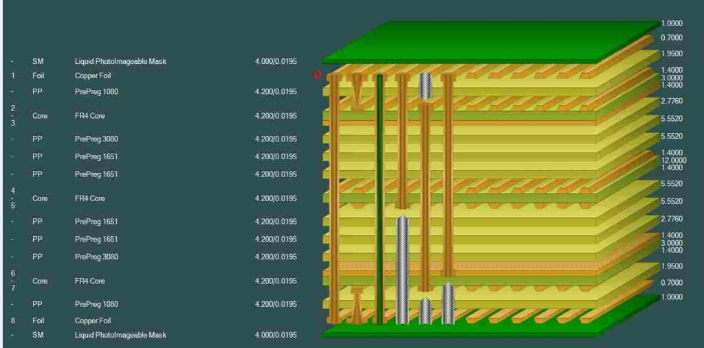
HDI PCB Manufacturing Capabiltiy : 1+N+1, 2+N+2, 3+N+3,4+N+4, 5+N+5, any layer in R&D.
| Feature | HDI technical CAPABILITIES |
| Number of layers | 4 – 32 layers standard, 56 layers advanced |
| Technology highlights | Multilayer boards with a higher connection pad density than standard boards, with finer lines/spaces, smaller via holes and capture pads allowing microvias to only penetrate select layers and also be placed in surface pads. |
| HDI builds | 1+N+1, 2+N+2, 3+N+3,4+N+4,5+N+5, any layer / ELIC, Ultra HDI in R&D |
| Materials | FR4 standard, FR4 high performance, Halogen free FR4, Rogers |
| Copper weights (finished) | 18μm – 70μm |
| Minimum track and gap | 0.075mm / 0.075mm |
| PCB thickness | 0.40mm – 3.20mm |
| Maxmimum dimensions | 610mm x 450mm; dependant upon laser drilling machine |
| Surface finishes available | OSP, Enepig, ENIG, Immersion tin, Immersion silver, Electrolytic gold, Gold fingers |
| Minimum mechanical drill | 0.15mm |
| Minimum laser drill | 0.10mm standard, 0.075mm advanced |