Understanding Common PCB Soldering Defects
Printed circuit boards (PCBs) are essential components in modern electronics. Proper soldering is crucial for ensuring the reliability and functionality of these boards. However, various defects can occur during the soldering process, leading to issues in the final product. In this article, we will explore the common types of PCB Soldering Defects, their causes, and methods for prevention and repair.
Types of PCB Soldering Defects
There are several types of soldering defects that can occur on PCBs. Some of the most common include:
- Bridging: Unwanted solder connections between adjacent pins or traces.
- Cold joints: Dull, grainy, or incomplete solder joints due to insufficient heat or poor wetting.
- Insufficient solder: Lack of solder, resulting in weak or unstable connections.
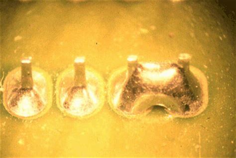
- Excessive solder: Excess solder, potentially causing short circuits or impeding component placement.
- Solder Balls: Small spheres of solder that can cause short circuits if they come into contact with other components or traces.
- Tombstoning: Components standing on end due to uneven heating or surface tension during reflow soldering.
- Lifted pads: Pads that have separated from the PCB Substrate due to excessive heat or mechanical stress.
Causes of PCB Soldering Defects
Several factors can contribute to the occurrence of soldering defects on PCBs:
- Improper temperature: Insufficient or excessive heat during the soldering process.
- Poor solder wetting: Inadequate flux or contaminated surfaces preventing proper solder adhesion.
- Incorrect solder composition: Using solder with the wrong alloy or impurities.
- Mechanical stress: Applying excessive force or bending the PCB during soldering or handling.
- Inadequate cleaning: Failing to remove flux residue or other contaminants before or after soldering.
- Operator error: Lack of skill, experience, or attention to detail by the person performing the soldering.
Preventing PCB Soldering Defects
Prevention is key when it comes to minimizing soldering defects on PCBs. Here are some best practices to follow:
Proper Material Selection
- Choose high-quality PCB substrates with suitable surface finishes.
- Use solder alloys with the appropriate composition and melting temperature for the application.
- Select flux that is compatible with the solder alloy and PCB Surface Finish.
Optimal Process Parameters
- Set and maintain the correct soldering temperature for the specific solder alloy and PCB materials.
- Control the soldering time to ensure adequate heat transfer without causing damage.
- Adjust the soldering iron tip size and shape to match the component and pad sizes.
Cleanliness and Contamination Control
- Clean the PCB and components thoroughly before soldering to remove oxides, dirt, and grease.
- Use appropriate cleaning agents and methods to remove flux residue after soldering.
- Maintain a clean and organized work environment to minimize the risk of contamination.
Operator Training and Skill Development
- Provide comprehensive training to operators on soldering techniques, best practices, and defect recognition.
- Encourage continuous skill development and provide ongoing training as needed.
- Implement a quality control process to monitor and provide feedback on operator performance.

Repairing PCB Soldering Defects
Despite best efforts to prevent defects, they may still occur. When faced with soldering defects, there are several methods for repair:
Rework Techniques
- Desoldering: Removing the defective solder joint using desoldering tools such as wick, pumps, or hot air.
- Resoldering: Applying fresh solder to the joint after cleaning the area and ensuring proper wetting.
- Component replacement: Removing the defective component and replacing it with a new one.
- Pad repair: Rebuilding lifted or damaged pads using specialized repair materials and techniques.
Inspection and Quality Control
- Visually inspect the PCB for defects using magnification tools or automated optical inspection (AOI) systems.
- Use electrical testing methods such as in-circuit testing (ICT) or flying probe testing to verify proper connections and functionality.
- Implement a quality control process to identify and address defects before the PCB is assembled into the final product.
| Defect Type | Causes | Prevention | Repair |
|---|---|---|---|
| Bridging | Excessive solder, incorrect tip size | Proper solder amount, appropriate tip size | Desolder and resolder |
| Cold joints | Insufficient heat, poor wetting | Optimal temperature, clean surfaces | Resolder with proper technique |
| Insufficient solder | Inadequate solder, poor wetting | Proper solder amount, clean surfaces | Add more solder |
| Excessive solder | Excessive solder, incorrect tip size | Proper solder amount, appropriate tip size | Desolder excess solder |
| Solder balls | Excessive solder, contamination | Proper solder amount, clean surfaces | Remove solder balls, clean area |
| Tombstoning | Uneven heating, surface tension | Balanced heating, proper reflow profile | Resolder with even heating |
| Lifted pads | Excessive heat, mechanical stress | Controlled temperature, gentle handling | Pad repair or replacement |

Frequently Asked Questions (FAQ)
1. What is the most common type of PCB soldering defect?
Cold joints are one of the most common soldering defects. They occur when there is insufficient heat or poor wetting, resulting in a dull, grainy, or incomplete solder joint.
2. Can PCB soldering defects be completely eliminated?
While it may not be possible to completely eliminate all soldering defects, following best practices in material selection, process control, cleanliness, and operator training can significantly minimize their occurrence.
3. How can I identify PCB soldering defects?
Visual inspection using magnification tools or automated optical inspection (AOI) systems is the primary method for identifying soldering defects. Electrical testing methods such as in-circuit testing (ICT) or flying probe testing can also help detect defects that affect functionality.
4. Is it always necessary to repair PCB soldering defects?
The decision to repair a soldering defect depends on the severity and potential impact on the PCB’s functionality and reliability. Some minor defects may not require repair, while others can cause significant issues if left unaddressed.
5. Can soldering defects be repaired by someone without professional training?
While some basic soldering defects may be repairable by individuals with soldering experience, more complex defects often require the skills and knowledge of trained professionals. Attempting repairs without proper training can potentially cause further damage to the PCB.

Conclusion
PCB soldering defects can have significant impacts on the reliability and functionality of electronic devices. Understanding the common types of defects, their causes, and methods for prevention and repair is essential for anyone involved in PCB manufacturing or assembly. By implementing best practices in material selection, process control, cleanliness, and operator training, the occurrence of soldering defects can be minimized. When defects do occur, careful inspection and appropriate repair techniques can help salvage the affected PCBs and ensure the final product meets the required quality standards.


Leave a Reply