PCB Blog
-
Read more: Does a blind hole go all the way through the metal?
Understanding Blind Holes A blind hole is a hole that does not go all the way through the material it is drilled into. It is a recess or void that has a closed bottom. In machining and manufacturing, blind holes are used to create threaded holes for screws or bolts, […]
-
 Read more: Does a blind hole go all the way through the metal?
Understanding blind holes and through holes When working with metal parts that require holes to be drilled or machined, there are two main types of holes – blind holes and through holes. The key difference between these two hole types comes down to how far they extend through the thickness […]
-
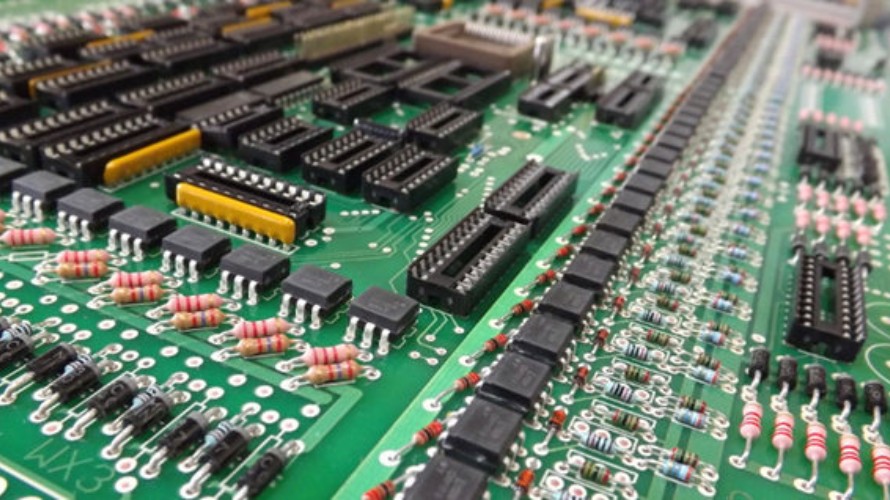
Why are Through Holes Preferred to Blind Holes?
Posted by
–
 Read more: Why are Through Holes Preferred to Blind Holes?
Introduction In manufacturing and engineering, holes are required in parts and components for various reasons like fastening, locating, alignment, weight reduction etc. Holes can be broadly classified into two categories – through holes and blind holes. As the names suggest, a through hole passes completely through the workpiece, while a […]
-
Are blind vias more expensive?
Posted by
–
 Read more: Are blind vias more expensive?
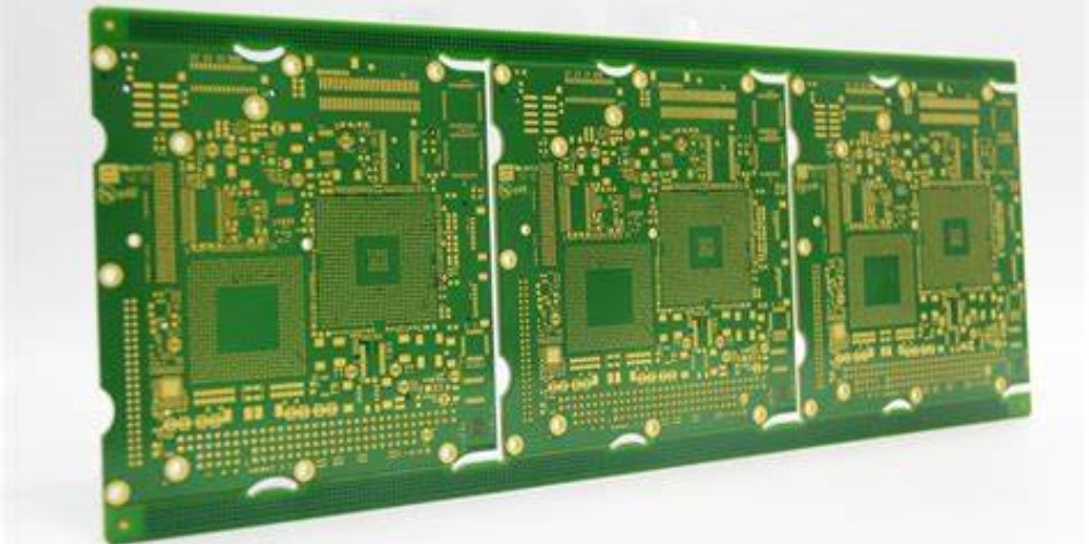
Introduction A via is a small hole that is drilled in a printed circuit board (PCB) and plated with a metal coating to electrically connect different layers together. Vias come in two main types – through-hole vias that span all layers of the PCB from top to bottom, and blind/buried […]
-
 Read more: What is the difference between blind and through-hole vias?
Vias are conductive holes used in printed circuit boards (PCBs) to connect different layers of the board together. There are two main types of vias – blind vias and through-hole vias. The key differences between blind and through-hole vias are: Blind Vias Blind vias connect one or more internal PCB […]
-
What is a Blind Circuit?
Posted by
–
 Read more: What is a Blind Circuit?
A blind circuit, also known as an unloaded circuit, refers to an electrical circuit that does not have an electrical load connected to it. In other words, a blind circuit is a complete conducting path without any devices that use the electricity. Blind circuits are commonly used for testing purposes […]
-
Why use blind vias?
Posted by
–
 Read more: Why use blind vias?
What are blind vias? Blind vias, also known as buried vias, are holes that connect different layers of a printed circuit board (PCB) without being visible or accessible from the surface of the board. The via is plated through, allowing electric currents to flow between layers, but the ends are […]
-
What is Blind Via in PCB?
Posted by
–
 Read more: What is Blind Via in PCB?
Introduction In printed circuit boards (PCBs), a blind via is a hole that connects different layers of a multi-layer PCB without going through the entire board. Blind vias are used to route connections between internal layers of a PCB without using up space on the outer layers. They allow designers […]
-
What is the difference between HDI and PCB?
Posted by
–
 Read more: What is the difference between HDI and PCB?
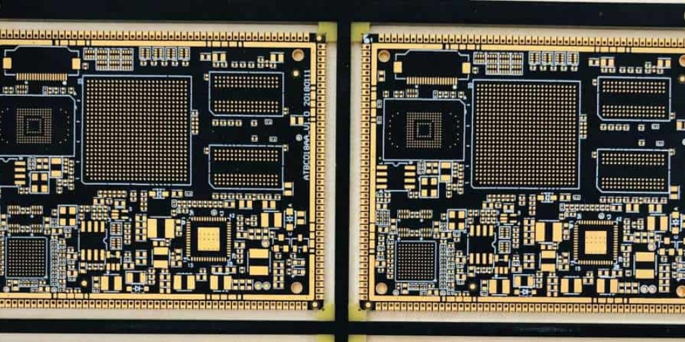
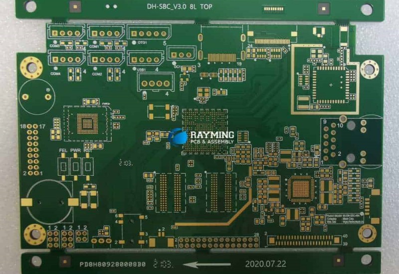
Introduction Printed circuit boards (PCBs) and high-density interconnect (HDI) PCBs are key components in modern electronics. They provide the foundation for mounting and connecting electronic components. While they share some similarities, there are important differences between traditional PCBs and HDI PCBs related to their design, manufacturing, and use. This article […]
-
What is HDI high density interconnect?
Posted by
–
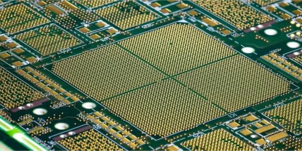
Read more: What is HDI high density interconnect?Introduction HDI (High Density Interconnect) is a printed circuit board (PCB) technology that enables higher interconnect density and thinner circuit boards compared to conventional PCB technologies. HDI allows tracing spacing and via diameters to be reduced, resulting in more routing channels and higher component densities. This enables more functionality to […]


