PCB Blog
-
What is a Printed Circuit Board?
Posted by
–
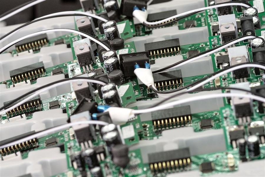
Read more: What is a Printed Circuit Board?A printed circuit board (PCB) is a board used to mechanically support and electrically connect electronic components using conductive pathways or traces etched from copper sheets laminated onto a non-conductive substrate. PCBs provide the necessary electrical connections between components to form functional electronic circuits and are found in almost all modern electronic devices. History of…
-
Is Via Bad for PCB?
Posted by
–
 Read more: Is Via Bad for PCB?
Introduction A printed circuit board (PCB) serves as the foundation for almost all modern electronics. It provides the mechanical structure and electrical connections between components. Vias play a critical role in allowing signals and power to be routed between layers in multilayer PCBs. However, there has been some debate around whether vias have detrimental effects…
-
Why avoid vias?
Posted by
–
 Read more: Why avoid vias?
Introduction In printed circuit board (PCB) design, vias are plated through-holes that provide electrical connections between different copper layers. While vias are essential components in complex PCBs, designers often try to minimize and avoid using unnecessary vias. This article explores the reasons why engineers aim to reduce vias, the problems vias can cause, and guidelines…
-
Are Blind Vias Filled?
Posted by
–
 Read more: Are Blind Vias Filled?
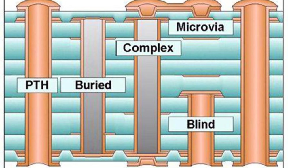
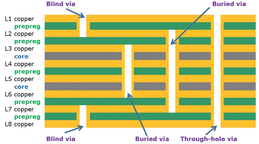
Introduction In printed circuit board (PCB) design, vias are plated-through holes that connect traces between layers. Vias can be classified as through vias or blind/buried vias. Through vias span the entire height of the PCB, connecting layers from the top to the bottom. Blind or buried vias, on the other hand, connect only between adjacent…
-
Which type of vias not visible from outside?
Posted by
–
 Read more: Which type of vias not visible from outside?
Introduction Vias are plated through holes in printed circuit boards (PCBs) that provide electrical connections between different layers in the board. There are several types of vias, and some are designed to not be visible from the outside of the PCB. In this article, we will discuss the different types of vias and which ones…
-
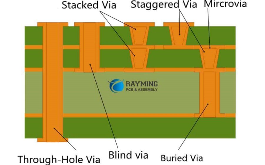 Read more: What are blind and buried vias compared to normal vias?
Vias are conductive holes in a printed circuit board (PCB) that allow connections between different layers. There are a few different types of vias: Normal Vias Normal vias are the most common type of via used in PCBs. They connect two or more layers vertically by forming a conductive path through the entire board. Features:…
-
How are Buried Vias Plated?
Posted by
–
 Read more: How are Buried Vias Plated?
Buried vias are an important component in printed circuit boards (PCBs) that allow connections between different layers in the board. Plating of buried vias is a key process that ensures reliable connectivity and allows the vias to serve their purpose. Here is an overview of how buried vias are plated during PCB fabrication. What are…
-
Are buried vias filled?
Posted by
–
 Read more: Are buried vias filled?
Buried vias are an important component in printed circuit boards (PCBs) that allow connections between different layers in the board. A key question that arises is whether these vias are filled or unfilled. The answer has implications for manufacturability, reliability, and performance of the PCB. This article provides an in-depth look at buried vias, whether…
-
 Read more: What is the difference between Microvia and buried via?
Introduction Printed circuit boards (PCBs) are integral components of most electronic devices. They provide the physical platform to mount and interconnect electronic components using conductive copper tracks. To connect different layers in a multilayer PCB, vertical interconnects called vias are used. The two main types of vias used in PCBs are microvias and buried vias.…
-
What is buried vias in PCB?
Posted by
–
Read more: What is buried vias in PCB?Introduction Printed circuit boards (PCBs) are the backbone of modern electronics. They provide the electrical connections and pathways between components mounted on the board. To connect components and routing signals between layers of the PCB, plated through holes called vias are used. Vias can be through-hole vias that span the entire thickness of the PCB…


