PCB Blog
-
What are Buried Vias?
Posted by
–
 Read more: What are Buried Vias?
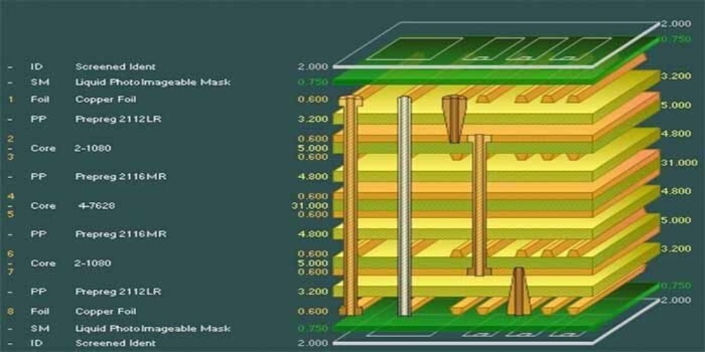
Introduction to Buried Vias Buried vias are a type of via connection used in printed circuit boards (PCBs) to connect different layers of a multilayer PCB. Vias are plated through holes that allow traces on different layers to be electrically connected. In a typical via, the hole is plated through […]
-
What is the size of blind via?
Posted by
–
 Read more: What is the size of blind via?
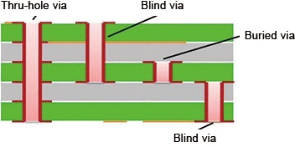
Introduction A blind via is a hole that connects different layers of a printed circuit board (PCB) together electrically without having a pad on the external layers. Blind vias are often used to route connections between inner layers of a multilayer PCB while keeping the outer surfaces free of vias […]
-
Do vias increase PCB cost?
Posted by
–
 Read more: Do vias increase PCB cost?
Vias are metalized holes that allow connections between different layers of a printed circuit board (PCB). They provide vertical interconnects to route signals between layers and connect surface mounted components to inner layer traces. While essential for routing and connectivity, vias also impact the overall cost of PCB fabrication and […]
-
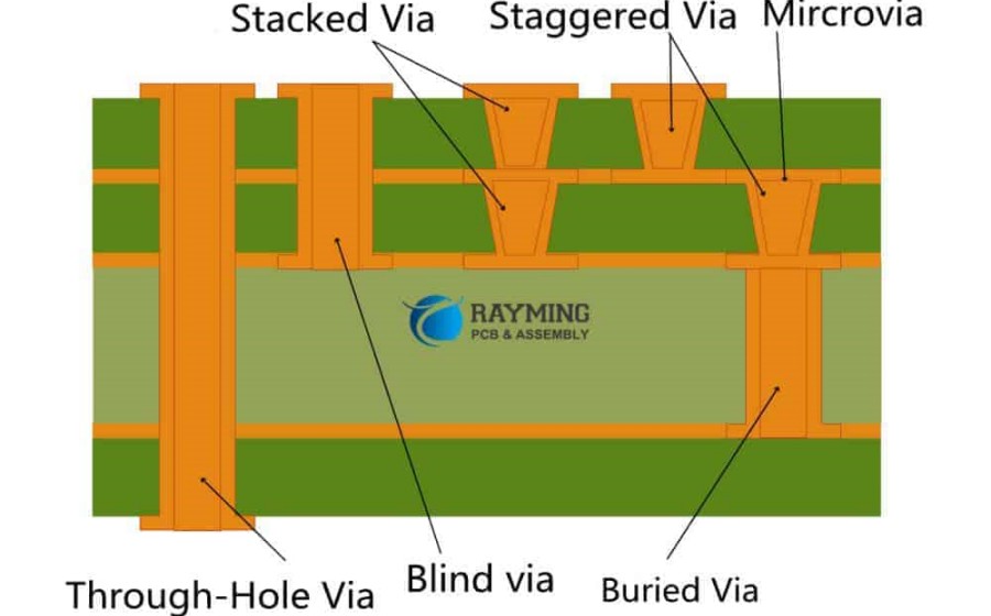 Read more: What is the difference between a via-in-PAD and a Microvia?
Introduction to microvias and their various types The continuous miniaturization of electronics has led to shrinking component sizes and PCB features. As a result, the via structure, which provides the electrical interconnect between the various layers of a printed circuit board (PCB), has also evolved over the years. Some of […]
-
Can I put vias on pads?
Posted by
–
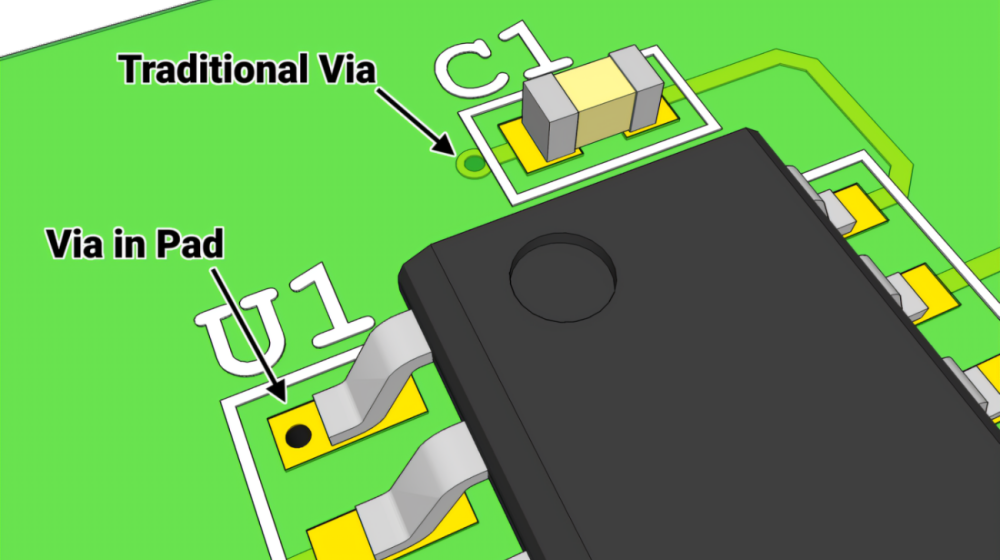 Read more: Can I put vias on pads?
Introduction When designing printed circuit boards (PCBs), vias and pads are two important features that enable connections between different layers of the board. A via is a plated through hole that connects two or more layers in the PCB, while a pad is the metal surface onto which components are […]
-
Do blind vias cost more?
Posted by
–
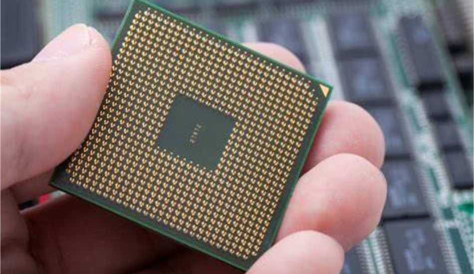 Read more: Do blind vias cost more?
Blind vias are an important component in printed circuit board (PCB) design and manufacturing. As the name suggests, blind vias connect layers on a PCB without going all the way through from the top to the bottom. Understanding the costs associated with blind vias is key for PCB designers and […]
-
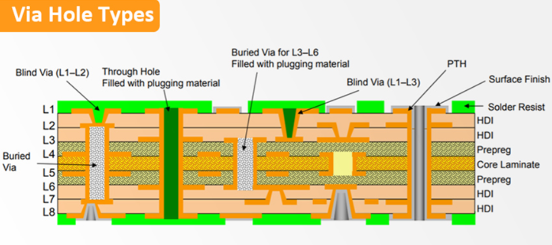 Read more: What is the difference between blind via and Microvia?
Introduction Printed circuit boards (PCBs) contain vias to provide electrical connections between different layers of the board. Vias are plated-through holes that allow signals to travel in the Z-axis between layers. There are two main types of vias used in PCBs – blind vias and microvias. Both provide interlayer connections […]
-
Read more: What is the difference between blind via and via in pad?
Introduction When designing printed circuit boards (PCBs), vias play an important role in connecting different layers and routing signals. There are two main types of vias – blind vias and vias in pads. Understanding the difference between these two via types and when to use each is crucial for optimizing […]
-
What is the use of blind vias?
Posted by
–
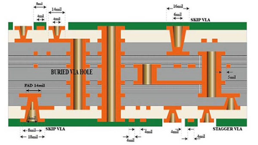 Read more: What is the use of blind vias?
Introduction A via is a conductive hole that connects different layers of a printed circuit board (PCB). Vias allow signals to travel between layers. There are several types of vias: Blind vias are widely used in complex, multilayer PCBs as they offer several advantages over through-hole vias: Key Advantages of […]
-
What is the tap depth for blind holes?
Posted by
–
 Read more: What is the tap depth for blind holes?
When machining metal parts, holes are often drilled and then threaded with taps to create internal threads so that screws or bolts can be used to fasten parts together. Blind holes are holes that do not pass fully through the workpiece. Determining the appropriate tap depth is important for blind […]
