1. Optimize Solder Paste Printing Parameters
Proper solder paste printing is the foundation for Avoiding Solder Balls. Key parameters to optimize include:
- Stencil thickness: Use a stencil thickness that matches the solder paste particle size and desired deposit height. Typically, a thinner stencil (4-5 mils) is recommended for fine-pitch components.
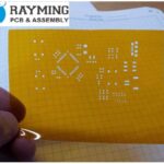
- Aperture size and shape: Ensure aperture openings are slightly larger than the pad size to allow for proper paste release. Rounded or tapered aperture walls can improve paste transfer.
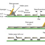
- Print speed and pressure: Adjust print speed and pressure to achieve a consistent, uniform solder paste deposit. Slower print speeds and lower pressures are generally better for fine-pitch printing.
| Pitch | Stencil Thickness | Aperture Size | Print Speed | Pressure |
|---|---|---|---|---|
| ≥ 0.65 mm | 5-6 mils | Pad + 10-20% | 25-50 mm/s | 6-8 kg |
| 0.5-0.65 mm | 4-5 mils | Pad + 5-10% | 25-40 mm/s | 5-7 kg |
| ≤ 0.5 mm | 3-4 mils | Pad size | 20-30 mm/s | 4-6 kg |
Table 1. Recommended solder paste printing parameters based on component pitch.
2. Use High-Quality Solder Paste
Selecting a high-quality solder paste is crucial for minimizing solder balls. Look for solder pastes with the following characteristics:
- Consistent particle size distribution: Pastes with a narrow particle size range will print more consistently and be less prone to solder balling.
- Low oxide content: Solder pastes with low oxide levels will have better wetting properties and be less likely to form solder balls.
- Appropriate flux activity: Choose a solder paste with a flux that matches your specific application requirements (e.g., no-clean, water-soluble, or RMA).
3. Maintain Proper Stencil Cleaning
Regular stencil cleaning is essential for maintaining print quality and preventing solder balls. Implement the following cleaning practices:
- Underside cleaning: Clean the underside of the stencil after every print to remove any solder paste residue that could lead to solder balling.
- Periodic full cleaning: Perform a thorough cleaning of both sides of the stencil at regular intervals (e.g., every 4-8 hours) to prevent paste buildup.
- Use appropriate cleaning agents: Select cleaning agents that are compatible with your solder paste chemistry and effectively remove residues without damaging the stencil.

4. Control Solder Paste Storage and Handling
Proper storage and handling of solder paste can help prevent solder balling issues:
- Refrigeration: Store solder paste in a refrigerator at the manufacturer-recommended temperature (typically 0-10°C) to slow down oxidation and maintain paste consistency.
- Warm-up time: Allow solder paste to reach room temperature before use (usually 2-4 hours) to ensure optimal performance.
- Shelf life: Use solder paste within its specified shelf life to avoid degradation that could lead to solder balling.
- Handling: Minimize the time solder paste is exposed to air and avoid contamination by using clean spatulas and keeping containers sealed when not in use.
5. Optimize Reflow Profile
An optimized reflow profile is critical for minimizing solder balls. Key aspects to consider include:
- Preheat rate: Use a gradual preheat rate (1-3°C/s) to evaporate solvents and avoid Solder Paste Slumping or splattering, which can cause solder balls.
- Peak temperature: Ensure the peak temperature is high enough to fully melt the solder paste (typically 20-30°C above the solder liquidus temperature) but not so high that it causes solder balling or component damage.
- Time above liquidus (TAL): Maintain sufficient TAL (60-90 seconds) to allow for complete solder wetting and intermetallic formation while minimizing the risk of solder balling.
- Cooling rate: Control the cooling rate (2-4°C/s) to promote proper solder joint solidification and prevent solder balling due to thermal shock.
| Profile Parameter | Recommendation |
|---|---|
| Preheat Rate | 1-3°C/s |
| Peak Temperature | Liquidus + 20-30°C |
| Time Above Liquidus | 60-90 seconds |
| Cooling Rate | 2-4°C/s |
Table 2. Recommended reflow profile parameters for minimizing solder balls.
6. Maintain Proper PCB Cleanliness
A clean PCB surface is essential for preventing solder balls. Implement the following PCB cleaning practices:
- Pre-soldering cleaning: Clean PCBs before solder paste printing to remove any contaminants, such as dirt, dust, or oils, that could cause solder balling.
- Handling: Handle PCBs with gloves to avoid introducing skin oils or other contaminants that could lead to solder balling.
- Storage: Store PCBs in a clean, dry environment to prevent contamination and oxidation that could contribute to solder balling.
7. Use Nitrogen in Reflow Oven
Using nitrogen in the reflow oven can help reduce solder balling by minimizing oxidation during the soldering process. Benefits of nitrogen reflow include:
- Reduced oxide formation: Nitrogen creates an inert atmosphere that prevents solder paste and PCB surface oxidation, reducing the likelihood of solder balling.
- Improved wetting: By minimizing oxidation, nitrogen promotes better solder wetting and flow, resulting in fewer solder balls.
- Enhanced joint appearance: Nitrogen reflow produces shinier, smoother solder joints with fewer surface defects, such as solder balls.
8. Implement SPI and AOI Inspection
Solder paste inspection (SPI) and automated optical inspection (AOI) can help identify potential solder balling issues early in the assembly process:
- SPI: Use SPI to verify solder paste deposit volume, height, and shape before reflow. Detecting and correcting paste printing issues can prevent solder balling downstream.
- AOI: Implement AOI after reflow to detect solder balls and other soldering defects. Catching solder balls early allows for timely process adjustments and rework.
9. Control Component Placement Accuracy
Accurate component placement is crucial for minimizing solder balls:
- Pick-and-place machine calibration: Regularly calibrate pick-and-place machines to ensure precise component placement and avoid misalignment that could lead to solder balling.
- Component packaging: Use high-quality, properly sealed component packaging to prevent contamination and ensure consistent pick-and-place performance.
- Nozzle maintenance: Clean and inspect pick-and-place nozzles regularly to ensure accurate component handling and placement.
10. Manage PCB Warpage
PCB warpage can contribute to solder balling by creating uneven surfaces that disrupt solder paste printing and reflow. To manage PCB warpage:
- Material selection: Choose PCB materials with low coefficients of thermal expansion (CTE) to minimize warpage during reflow.
- Balanced copper distribution: Design PCBs with balanced copper distribution on all layers to reduce thermal stress and warpage.
- Support pins or inserts: Use support pins or inserts in the conveyor system to minimize PCB warpage during reflow.
11. Continuously Monitor and Improve Processes
Continuously monitoring and improving your SMT processes is key to avoiding solder balls and maintaining high-quality PCBA production:
- Statistical process control (SPC): Implement SPC to track key process parameters, identify trends, and make data-driven improvements.
- Regular maintenance: Perform regular maintenance on all equipment, including printers, pick-and-place machines, and reflow ovens, to ensure consistent performance and minimize solder balling risks.
- Training: Provide ongoing training for operators and technicians to ensure adherence to best practices and promote a quality-focused culture.
By following these 11 easy steps, you can significantly reduce the occurrence of solder balls in your SMT manufacturing process, resulting in higher-quality, more reliable PCBAs.
Frequently Asked Questions
1. What causes solder balls in SMT assembly?
Solder balls can be caused by various factors, including:
– Improper solder paste printing (e.g., excessive paste, uneven deposits)
– Solder paste contamination or degradation
– PCB surface contamination or oxidation
– Incorrect reflow profile (e.g., excessive peak temperature, insufficient cooling rate)
– Component placement inaccuracies
– PCB warpage
2. How can I tell if my solder paste is causing solder balls?
Signs that your solder paste may be contributing to solder balls include:
– Inconsistent or uneven paste deposits
– Paste slumping or splattering during reflow
– Solder balls forming primarily on paste deposits rather than other areas of the PCB
– Increased solder ball occurrence after changing paste brands or batches
If you suspect your solder paste is causing solder balls, try using a different paste with a finer particle size, lower oxide content, or more suitable flux activity for your application.
3. Can solder balls be reworked?
Yes, solder balls can be reworked using various methods, such as:
– Manual removal with tweezers or a soldering iron
– Solder wick to absorb excess solder
– Localized hot air rework to reflow and remove solder balls
– Automated rework systems for more complex or high-volume rework
However, preventing solder balls through process optimization is always preferable to rework, as rework can be time-consuming, costly, and potentially damaging to the PCBA.
4. How does nitrogen reflow help prevent solder balls?
Nitrogen reflow helps prevent solder balls by creating an inert atmosphere in the reflow oven. This inert atmosphere minimizes oxidation of the solder paste and PCB surface during the reflow process. By reducing oxidation, nitrogen reflow promotes better solder wetting and flow, resulting in fewer solder balls and improved joint appearance.
5. What role does PCB design play in avoiding solder balls?
PCB design can influence the occurrence of solder balls in several ways:
– Pad size and shape: Properly sized and shaped pads ensure adequate solder paste deposition and prevent solder balling due to insufficient or excessive paste coverage.
– Solder mask design: A well-designed solder mask helps contain solder paste and prevent bridging or solder balling between adjacent pads.
– Copper balance: Balancing copper distribution across PCB layers minimizes warpage during reflow, reducing the risk of solder balling due to uneven surfaces.
– Component selection: Choosing components with compatible packaging and termination materials can help prevent solder balling caused by thermal mismatches or contamination.
By considering these design factors and collaborating closely with your PCB fabricator and assembly partner, you can create PCB designs that are more resistant to solder balling and other SMT defects.
In conclusion, avoiding solder balls in SMT manufacturing requires a comprehensive approach that addresses multiple aspects of the assembly process, from solder paste selection and printing to reflow profiling and PCB design. By implementing the 11 easy steps outlined in this guide and staying vigilant in monitoring and improving your processes, you can significantly reduce the occurrence of solder balls and produce higher-quality, more reliable PCBAs.
Leave a Reply