Introduction to PCB Holes
Printed Circuit Boards (PCBs) are essential components in modern electronics, providing a platform for electrical connections and mechanical support for various components. One crucial aspect of PCB design and manufacturing is the creation of holes. PCB holes serve multiple purposes, including component mounting, electrical connectivity, and heat dissipation. In this article, we will explore the different types of PCB Drilled Holes, their characteristics, and their applications.
Types of PCB Holes
Through Holes
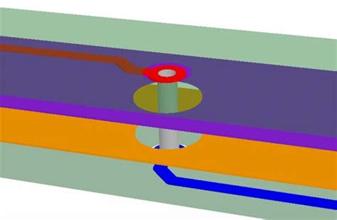
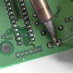
Through holes are the most common type of PCB holes. They are drilled completely through the PCB, creating a hole that extends from the top layer to the bottom layer. Through holes are typically used for mounting through-hole components, such as resistors, capacitors, and connectors. They also facilitate electrical connectivity between layers of the PCB.
Characteristics of Through Holes
- Drilled completely through the PCB
- Used for mounting through-hole components
- Provide electrical connectivity between layers
- Typically plated with conductive material
Applications of Through Holes
- Through-hole component mounting
- Electrical connectivity between layers
- Mechanical support for components
Blind Vias
Blind vias are holes that are drilled from one side of the PCB and terminate at a specific inner layer without reaching the opposite side. They are used to establish electrical connections between the surface layer and one or more inner layers of the PCB. Blind vias are commonly employed in high-density PCB designs to save space and improve signal integrity.
Characteristics of Blind Vias
- Drilled from one side of the PCB
- Terminate at a specific inner layer
- Used for electrical connections between surface and inner layers
- Require precise depth control during drilling
Applications of Blind Vias
- High-density PCB designs
- Establishing electrical connections between surface and inner layers
- Saving space on the PCB surface
Buried Vias
Buried vias are holes that are drilled between inner layers of the PCB and do not extend to either the top or bottom surface. They are used to create electrical connections between inner layers without occupying space on the outer layers. Buried vias are typically employed in complex, Multi-Layer PCB designs to optimize signal routing and reduce electromagnetic interference (EMI).
Characteristics of Buried Vias
- Drilled between inner layers of the PCB
- Do not extend to the top or bottom surface
- Used for electrical connections between inner layers
- Require precise alignment and registration during PCB fabrication
Applications of Buried Vias
- Complex, multi-layer PCB designs
- Optimizing signal routing
- Reducing electromagnetic interference (EMI)
- Saving space on the outer layers of the PCB
Micro Vias
Micro vias are tiny holes with diameters typically less than 0.15mm (6 mils). They are used in high-density interconnect (HDI) PCB designs to establish fine-pitch connections between layers. Micro vias are created using specialized laser drilling techniques, enabling precise and accurate hole formation.
Characteristics of Micro Vias
- Tiny holes with diameters less than 0.15mm
- Used in high-density interconnect (HDI) PCB designs
- Created using laser drilling techniques
- Enable fine-pitch connections between layers
Applications of Micro Vias
- High-density interconnect (HDI) PCB designs
- Fine-pitch component mounting
- Establishing precise electrical connections between layers
- Miniaturization of electronic devices
Plated Through Holes (PTH)
Plated through holes (PTH) are through holes that are plated with a conductive material, typically copper, to create electrical connections between layers. The plating process involves depositing a thin layer of copper on the walls of the drilled hole, ensuring reliable electrical conductivity. PTH is widely used in PCB manufacturing for component mounting and establishing electrical connections.
Characteristics of Plated Through Holes
- Through holes plated with a conductive material (usually copper)
- Create electrical connections between layers
- Provide mechanical support for components
- Require precise plating process control
Applications of Plated Through Holes
- Component mounting (through-hole components)
- Establishing electrical connections between layers
- Providing mechanical stability to the PCB Assembly
Non-Plated Through Holes (NPTH)
Non-plated through holes (NPTH) are through holes that are not plated with a conductive material. They are used for various purposes, such as mechanical support, alignment, or mounting non-electrical components. NPTH are often employed in PCB designs where electrical connectivity is not required, and they can be created using standard drilling techniques.
Characteristics of Non-Plated Through Holes
- Through holes without conductive plating
- Used for mechanical support, alignment, or mounting non-electrical components
- Do not provide electrical connectivity
- Created using standard drilling techniques
Applications of Non-Plated Through Holes
- Mounting non-electrical components (e.g., spacers, standoffs)
- Alignment of PCB Layers or components
- Mechanical support for the PCB assembly
Hole Drilling Techniques
Mechanical Drilling
Mechanical drilling is the most common method for creating holes in PCBs. It involves using a drill bit to physically remove material from the PCB Substrate. Mechanical drilling is suitable for creating through holes, blind vias, and non-plated through holes. The process is relatively fast and cost-effective, making it widely used in PCB manufacturing.
Characteristics of Mechanical Drilling
- Uses a drill bit to remove material from the PCB substrate
- Suitable for creating through holes, blind vias, and non-plated through holes
- Fast and cost-effective drilling method
- Requires precise drill bit selection and machine setup
Applications of Mechanical Drilling
- Creating through holes for component mounting
- Drilling blind vias for inner layer connections
- Creating non-plated through holes for mechanical support or alignment
Laser Drilling
Laser drilling is an advanced technique used for creating micro vias and other precision holes in PCBs. It employs a focused laser beam to vaporize the PCB material, resulting in clean and accurate holes. Laser drilling is particularly useful for high-density PCB designs that require fine-pitch connections and precise hole formation.
Characteristics of Laser Drilling
- Uses a focused laser beam to vaporize PCB material
- Creates clean and accurate holes
- Suitable for creating micro vias and precision holes
- Enables high-density PCB designs with fine-pitch connections
Applications of Laser Drilling
- Creating micro vias for high-density interconnect (HDI) PCBs
- Drilling precise holes for fine-pitch component mounting
- Creating intricate hole patterns for specialized applications

Hole Plating Techniques
Electroplating
Electroplating is a common method used for plating through holes and vias in PCBs. It involves immersing the PCB in an electrolytic solution containing the desired plating material (usually copper). An electric current is applied, causing the plating material to deposit on the walls of the holes, creating a conductive layer.
Characteristics of Electroplating
- Immerses the PCB in an electrolytic solution
- Uses an electric current to deposit plating material on hole walls
- Creates a conductive layer in through holes and vias
- Provides reliable electrical connectivity between layers
Applications of Electroplating
- Plating through holes for component mounting
- Creating conductive vias for inter-layer connections
- Enhancing electrical conductivity and signal integrity
Electroless Plating
Electroless plating is an alternative method for plating through holes and vias in PCBs. Unlike electroplating, it does not require an external electric current. Instead, it relies on an autocatalytic chemical reaction to deposit the plating material on the hole walls. Electroless plating is often used for high-aspect-ratio holes or when a more uniform plating thickness is desired.
Characteristics of Electroless Plating
- Uses an autocatalytic chemical reaction to deposit plating material
- Does not require an external electric current
- Suitable for high-aspect-ratio holes
- Provides a more uniform plating thickness
Applications of Electroless Plating
- Plating high-aspect-ratio holes in multi-layer PCBs
- Achieving uniform plating thickness in through holes and vias
- Plating holes in non-conductive substrates
Design Considerations for PCB Holes
When designing PCBs, several factors must be considered to ensure the proper functioning and manufacturability of the holes. These considerations include hole size, aspect ratio, pad size, and drilling tolerances.
Hole Size
The hole size is a critical factor in PCB design, as it affects component compatibility, manufacturing feasibility, and electrical performance. The hole size should be chosen based on the component leads or pins that will be inserted into the holes. It is essential to follow the manufacturer’s recommendations and industry standards when selecting hole sizes.
Aspect Ratio
The aspect ratio of a hole refers to the ratio of its depth to its diameter. High-aspect-ratio holes, where the depth is much greater than the diameter, can pose challenges during drilling and plating processes. It is crucial to consider the aspect ratio when designing PCBs, especially for multi-layer boards, to ensure proper hole formation and plating coverage.
Pad Size
The pad size around a hole is another important consideration in PCB design. The pad provides a surface for soldering components and ensures reliable electrical connections. The pad size should be sufficient to accommodate the component leads or pins and allow for proper soldering. It is essential to follow the component manufacturer’s recommendations and industry standards when determining pad sizes.
Drilling Tolerances
Drilling tolerances refer to the acceptable variations in hole size, position, and shape during the PCB manufacturing process. It is crucial to specify appropriate drilling tolerances based on the PCB design requirements and manufacturing capabilities. Tighter tolerances may be necessary for high-density designs or critical applications, while looser tolerances can be acceptable for less demanding designs.
Frequently Asked Questions (FAQ)
-
What is the difference between a through hole and a via?
A through hole is a hole that extends from the top layer to the bottom layer of a PCB, while a via is a hole that connects two or more layers within the PCB. Through holes are typically used for mounting components, while vias are used for inter-layer electrical connections. -
Can micro vias be created using mechanical drilling?
Micro vias are typically created using laser drilling techniques due to their small size and precise requirements. Mechanical drilling may not be suitable for creating micro vias, as it has limitations in terms of hole size and accuracy. -
What is the purpose of plating through holes in PCBs?
Plating through holes in PCBs serves two main purposes: establishing electrical connections between layers and providing mechanical support for components. The conductive plating material, usually copper, ensures reliable electrical conductivity and helps secure the components to the PCB. -
How does the aspect ratio affect the drilling and plating processes?
High-aspect-ratio holes, where the depth is much greater than the diameter, can pose challenges during drilling and plating processes. Drilling high-aspect-ratio holes requires specialized equipment and techniques to ensure proper hole formation. Plating high-aspect-ratio holes can be difficult, as achieving uniform plating coverage along the entire depth of the hole becomes more challenging. -
What are the advantages of using laser drilling for PCB holes?
Laser drilling offers several advantages for PCB hole creation, including precise and accurate hole formation, the ability to create micro vias, and suitability for high-density PCB designs. Laser drilling enables the creation of clean and small holes, making it ideal for fine-pitch connections and intricate hole patterns.
Conclusion
PCB drilled holes play a vital role in the functionality and performance of electronic devices. Understanding the different types of PCB holes, their characteristics, and their applications is essential for effective PCB design and manufacturing. Through holes, blind vias, buried vias, micro vias, plated through holes, and non-plated through holes each serve specific purposes and require appropriate design considerations.
Hole drilling techniques, such as mechanical drilling and laser drilling, along with hole plating methods like electroplating and electroless plating, enable the creation of reliable and conductive holes in PCBs. Designers must consider factors such as hole size, aspect ratio, pad size, and drilling tolerances to ensure the proper functioning and manufacturability of PCBs.
As PCB technology continues to advance, the importance of optimizing hole design and manufacturing processes becomes increasingly critical. By leveraging the various types of PCB holes and their associated techniques, designers and manufacturers can create high-quality, reliable, and high-performance electronic devices that meet the ever-growing demands of the industry.
Leave a Reply