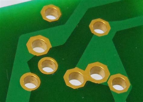
What are PCB Drilled Holes?
PCB drilled holes, also known as through-holes, are openings drilled through the printed circuit board (PCB) to allow for the connection of components on both sides of the board. These holes are essential for mounting and soldering various electronic components, such as resistors, capacitors, and integrated circuits (ICs), to the PCB. Drilled holes also serve as vias, which are used to connect different layers of a multi-layer PCB.
Types of PCB Drilled Holes
There are several types of PCB drilled holes, each serving a specific purpose:
-
Component Holes: These holes are used for mounting and soldering through-hole components to the PCB. The hole size depends on the lead diameter of the component.
-
Vias: Vias are used to connect different layers of a multi-layer PCB. There are three main types of vias:
- Through Vias: These vias go through all layers of the PCB.
- Blind Vias: These vias connect an outer layer to an inner layer, but do not go through the entire board.
-
Buried Vias: These vias connect inner layers without reaching the outer layers.
-
Mounting Holes: These holes are used for attaching the PCB to an enclosure or chassis using screws or standoffs.
-
Plated Holes: Plated holes have a conductive metal coating on the inside surface, allowing for electrical conductivity between layers.
-
Non-Plated Holes: Non-plated holes do not have a conductive coating and are used for mechanical purposes or as tooling holes.
Importance of Proper PCB Drilled Hole Design
Designing PCB drilled holes correctly is crucial for the following reasons:
-
Manufacturability: Proper hole design ensures that the PCB can be manufactured without issues, such as drill bit breakage or inaccurate hole placement.
-
Component Fit: Accurate hole sizes and placement guarantee that components can be easily inserted and soldered to the PCB.
-
Electrical Continuity: Plated holes must have the correct dimensions and plating thickness to ensure proper electrical conductivity between layers.
-
Mechanical Integrity: Mounting holes and vias should be designed to withstand mechanical stress and prevent PCB Delamination.

PCB Drilled Hole Design Considerations
When designing PCB drilled holes, consider the following factors:
Hole Size
The hole size should be appropriate for the component lead diameter or via requirements. Typically, the hole diameter is 0.2-0.5mm larger than the lead diameter to allow for easy insertion and proper soldering.
| Component Lead Diameter (mm) | Recommended Hole Diameter (mm) |
|---|---|
| 0.5 | 0.7 – 0.8 |
| 0.8 | 1.0 – 1.1 |
| 1.0 | 1.2 – 1.3 |
Hole Placement
Holes should be placed accurately to ensure proper component alignment and avoid conflicts with other PCB features, such as traces or planes. Maintain sufficient clearance between holes and other features to prevent manufacturing issues and electrical shorts.
Plating Thickness
For plated holes, the plating thickness should be sufficient to ensure electrical conductivity and mechanical strength. The typical copper plating thickness for PCB holes ranges from 20-35μm.
Aspect Ratio
The aspect ratio is the ratio of the hole depth to its diameter. High aspect ratios can lead to manufacturing challenges, such as incomplete plating or drill bit breakage. Generally, aim for an aspect ratio of 8:1 or less.

Common PCB Drilled Hole Issues and How to Avoid Them
-
Drill Bit Breakage: Caused by excessive aspect ratios, improper drill bit selection, or incorrect drilling parameters. To avoid this, follow the manufacturer’s guidelines for drill bit selection and drilling parameters, and keep aspect ratios within acceptable limits.
-
Incomplete Plating: Caused by high aspect ratios or inadequate cleaning of the holes before plating. Ensure proper cleaning processes are followed and keep aspect ratios within the recommended range.
-
Misaligned Holes: Caused by inaccurate CAD data or manufacturing errors. Double-check the CAD data for accuracy and work with reputable PCB Manufacturers who adhere to strict quality control processes.
-
Hole Wall Damage: Caused by aggressive drilling or inadequate support during drilling. Use appropriate drilling parameters and ensure the PCB is adequately supported during the drilling process.

FAQ
Q1: What is the difference between plated and non-plated holes?
A1: Plated holes have a conductive metal coating on the inside surface, allowing for electrical conductivity between layers. Non-plated holes do not have a conductive coating and are used for mechanical purposes or as tooling holes.
Q2: What is the recommended aspect ratio for PCB drilled holes?
A2: The recommended aspect ratio for PCB drilled holes is 8:1 or less to ensure manufacturability and avoid issues such as incomplete plating or drill bit breakage.
Q3: How do I determine the appropriate hole size for a component lead?
A3: The hole diameter should typically be 0.2-0.5mm larger than the component lead diameter to allow for easy insertion and proper soldering.
Q4: What are the different types of vias in a PCB?
A4: The three main types of vias are through vias (which go through all layers of the PCB), blind vias (which connect an outer layer to an inner layer), and buried vias (which connect inner layers without reaching the outer layers).
Q5: How can I avoid common PCB drilled hole issues?
A5: To avoid common issues, follow the manufacturer’s guidelines for drill bit selection and drilling parameters, keep aspect ratios within acceptable limits, ensure proper cleaning processes are followed, double-check CAD data for accuracy, and work with reputable PCB manufacturers who adhere to strict quality control processes.


Leave a Reply