What is PCB Prototyping?
PCB prototyping is the process of creating a functional prototype of a printed circuit board. This prototype is used to test and validate the design before moving to mass production. PCB prototyping involves several steps, including schematic design, PCB layout, fabrication, and assembly.
Why is PCB Prototyping Important?
PCB prototyping is critical for several reasons:
-
Design Validation: PCB prototyping allows designers to test and validate their designs before mass production. This helps identify any design flaws or issues early in the development process, saving time and money.
-
Functionality Testing: PCB Prototypes allow designers to test the functionality of their designs. This includes testing the electrical connections, component placement, and overall performance of the PCB.
-
Cost Savings: PCB prototyping can help save costs by identifying design flaws early in the development process. This prevents the need for costly redesigns and rework during mass production.
-
Time-to-Market: PCB prototyping can help reduce the time-to-market for electronic devices. By identifying and fixing design issues early, designers can move to mass production more quickly.
The 9 Fundamentals of PCB Prototyping and PCB Design Flow
1. Schematic Design
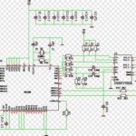
The first step in PCB prototyping is schematic design. This involves creating a diagram of the electrical connections and components needed for the PCB. The schematic design is created using Electronic Design Automation (EDA) software.
2. Component Selection
Once the schematic design is complete, the next step is to select the components needed for the PCB. This involves choosing the appropriate components based on their electrical and mechanical properties, as well as their cost and availability.
3. PCB Layout
After component selection, the next step is PCB layout. This involves arranging the components on the PCB and creating the copper traces that connect them. PCB layout is done using EDA software and requires careful consideration of signal integrity, power distribution, and thermal management.
4. Design Rule Check (DRC)
Before moving to fabrication, it is important to perform a Design Rule Check (DRC). This involves checking the PCB layout against a set of design rules to ensure that it meets the manufacturing requirements. The DRC helps identify any potential issues with the PCB layout, such as short circuits or insufficient clearances.
5. Gerber File Generation
Once the PCB layout is complete and has passed the DRC, the next step is to generate the Gerber files. Gerber files are the industry standard for PCB fabrication and contain all the information needed to manufacture the PCB, including the copper layers, drill holes, and silkscreen.
6. PCB Fabrication
With the Gerber files generated, the next step is PCB fabrication. This involves sending the Gerber files to a PCB manufacturer who will create the physical PCB. The fabrication process involves several steps, including:
- Copper Deposition: A layer of copper is deposited onto the PCB substrate.
- Photolithography: The copper layer is coated with a photoresist and exposed to UV light through a photomask. This creates the desired circuit pattern on the copper layer.
- Etching: The exposed copper is etched away, leaving only the desired circuit pattern.
- Drilling: Holes are drilled into the PCB for through-hole components and vias.
- Solder Mask Application: A layer of solder mask is applied to the PCB to protect the copper traces and prevent short circuits.
- Silkscreen Printing: The component labels and other markings are printed onto the PCB using silkscreen printing.
7. PCB Assembly
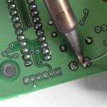
After PCB fabrication, the next step is PCB assembly. This involves soldering the components onto the PCB. There are two main methods of PCB assembly:
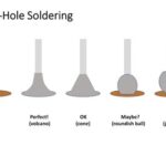
- Through-Hole Assembly: Through-hole components are inserted into holes drilled in the PCB and soldered onto the other side.
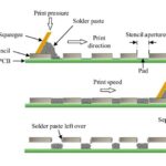
- Surface-Mount Assembly: Surface-mount components are placed onto pads on the surface of the PCB and soldered using a reflow oven.
8. Testing and Validation
Once the PCB is assembled, it is important to test and validate its functionality. This involves several types of testing, including:
- Visual Inspection: The PCB is visually inspected for any defects or issues, such as broken traces or poor solder joints.
- Electrical Testing: The PCB is tested for electrical continuity and functionality using test equipment such as multimeters and oscilloscopes.
- Functional Testing: The PCB is tested in its intended application to ensure that it performs as expected.
9. Iteration and Refinement
PCB prototyping is an iterative process. Based on the results of testing and validation, the PCB design may need to be refined and updated. This may involve changes to the schematic design, component selection, or PCB layout. The updated design is then sent back through the prototyping process until a final, functional prototype is achieved.

PCB Prototyping vs. PCB Mass Production
While PCB prototyping and mass production share many of the same steps, there are some key differences between the two processes:
| PCB Prototyping | PCB Mass Production |
|---|---|
| Small quantity (1-100 pieces) | Large quantity (100+ pieces) |
| Quick turnaround time (1-2 weeks) | Longer lead time (4-8 weeks) |
| Higher cost per unit | Lower cost per unit |
| More flexibility in design changes | Less flexibility in design changes |
| Used for testing and validation | Used for final production |
Frequently Asked Questions (FAQ)
- What is the difference between a PCB prototype and a final production PCB?
A PCB prototype is a functional version of the PCB used for testing and validation, while a final production PCB is the version used for mass production. PCB Prototypes may have lower quality materials and less stringent manufacturing tolerances compared to production PCBs.
- How long does PCB prototyping take?
The time required for PCB prototyping depends on the complexity of the design and the fabrication and assembly methods used. Typically, PCB prototyping can take anywhere from 1-2 weeks for simple designs to several weeks for more complex designs.
- What is the cost of PCB prototyping?
The cost of PCB prototyping depends on several factors, including the size and complexity of the PCB, the number of layers, and the quantity ordered. Typically, PCB prototyping can cost anywhere from a few hundred to several thousand dollars, depending on these factors.
- What are some common issues encountered during PCB prototyping?
Some common issues encountered during PCB prototyping include design errors, component availability issues, manufacturing defects, and assembly issues. These issues can be minimized through careful design, component selection, and testing.
- Can PCB prototyping be done in-house?
Yes, PCB prototyping can be done in-house using desktop PCB milling machines and manual assembly methods. However, for more complex designs or higher quantities, it is often more cost-effective to outsource PCB prototyping to a professional PCB manufacturer.
Conclusion
PCB prototyping is a critical step in the development of electronic devices. By following the nine fundamentals of PCB prototyping and PCB design flow, designers and engineers can create functional prototypes that validate their designs and identify any issues early in the development process. This helps save time, money, and ensures a smooth transition to mass production. With the right tools, processes, and partners, PCB prototyping can be a streamlined and efficient process that helps bring innovative electronic products to market faster.
Leave a Reply