What is a PCB Prototype?
A PCB (Printed Circuit Board) prototype is a preliminary version of a PCB design that is used for testing and validation before mass production. It is an essential step in the PCB manufacturing process as it allows designers and engineers to assess the functionality, reliability, and performance of the board.
PCB Prototypes are typically made in small quantities, ranging from a single board to a few dozen. They are often manufactured using different methods than the final production run, such as desktop CNC milling or 3D printing, to reduce costs and turnaround time.
Types of PCB Prototypes
There are several types of PCB prototypes, each serving a specific purpose in the design and testing process:
-
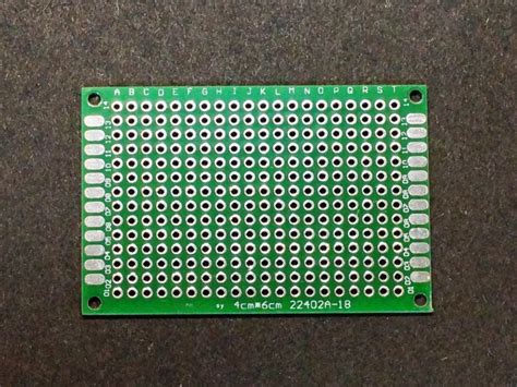
Visual Prototype: A non-functional board that represents the physical layout and appearance of the final PCB. It is used to check the dimensions, component placement, and overall aesthetics of the design.
-
Proof-of-Concept (PoC) Prototype: A functional board that demonstrates the basic functionality of the design. It may not include all the features or components of the final product but is used to validate the core concept.
-
Functional Prototype: A fully functional board that includes all the components and features of the final product. It is used for extensive testing and validation of the design before mass production.
PCB Prototype Manufacturing Methods
PCB prototypes can be manufactured using various methods, depending on the complexity of the design, the required turnaround time, and the available budget. Some common methods include:
-
CNC Milling: A subtractive process that uses a computer-controlled milling machine to remove copper from a blank PCB substrate, creating the desired circuit pattern.
-
3D Printing: An additive process that uses a 3D printer to deposit conductive and insulating materials layer by layer, creating a functional PCB.
-
Laser Etching: A process that uses a laser to remove the unwanted copper from a pre-sensitized PCB substrate, leaving the desired circuit pattern.
-
Chemical Etching: A traditional PCB manufacturing method that uses chemicals to remove the unwanted copper from a pre-sensitized PCB substrate.
| Manufacturing Method | Advantages | Disadvantages |
|---|---|---|
| CNC Milling | Fast turnaround, high precision, suitable for complex designs | Limited material options, higher cost for larger quantities |
| 3D Printing | Rapid prototyping, low cost for small quantities | Limited resolution and conductivity, slower for larger quantities |
| Laser Etching | High precision, fast turnaround | Limited material options, higher cost for larger quantities |
| Chemical Etching | Suitable for large quantities, wide range of materials | Slower turnaround, requires additional setup and tooling |
Why You Need a PCB Prototype
1. Design Validation
A PCB prototype allows you to validate your design before committing to mass production. By testing the prototype, you can identify and fix any design flaws, such as incorrect component placement, signal integrity issues, or power distribution problems. This helps to avoid costly mistakes and delays in the final production run.
2. Functionality Testing
With a functional PCB prototype, you can test the actual performance of your board under real-world conditions. This includes testing the board’s response to various inputs, outputs, and environmental factors, such as temperature, humidity, and vibration. By thoroughly testing the prototype, you can ensure that your final product will meet the desired specifications and performance requirements.
3. Compliance Testing
Many electronic products must comply with various industry standards and regulations, such as FCC (Federal Communications Commission) or CE (Conformité Européenne). A PCB prototype allows you to conduct compliance testing early in the development process, ensuring that your final product will meet the necessary regulatory requirements. This helps to avoid potential legal issues and costly redesigns later on.
4. Manufacturability Assessment
A PCB prototype can help you assess the manufacturability of your design. By working with a prototype, you can identify any potential manufacturing challenges, such as tight tolerances, difficult-to-source components, or complex assembly processes. This information can be used to optimize your design for manufacturing, reducing production costs and improving yields.
5. Investor and Customer Engagement
A functional PCB prototype can be a powerful tool for engaging investors and customers. By demonstrating a working product, you can showcase the capabilities and potential of your design, helping to secure funding or generate customer interest. A prototype can also be used for user testing and feedback, allowing you to refine your design based on real-world input.

The PCB Prototyping Process
The PCB prototyping process typically involves several steps, from design creation to final testing and validation. Here’s a general overview of the process:
-
Design Creation: The first step is to create the PCB design using EDA (Electronic Design Automation) software, such as Altium Designer, Eagle, or KiCad. This involves schematic capture, component selection, and PCB layout.
-
Design Review: Once the design is complete, it undergoes a thorough review process to ensure that it meets the desired specifications and design rules. This may involve collaboration with other team members, such as electrical engineers, mechanical engineers, and manufacturing experts.
-
Prototype Fabrication: After the design is finalized, the PCB prototype is fabricated using one of the methods discussed earlier, such as CNC milling or 3D printing. The choice of fabrication method depends on the complexity of the design, the required turnaround time, and the available budget.
-
Component Sourcing and Assembly: The necessary components are sourced and the prototype is assembled, either manually or using automated assembly equipment. This step may involve soldering, wire bonding, or other assembly techniques.
-
Testing and Validation: The assembled prototype undergoes various tests to validate its functionality, performance, and compliance with industry standards. This may include electrical testing, environmental testing, and software testing.
-
Design Iteration: Based on the results of the testing and validation phase, the design may be iterated and refined. This process may involve multiple rounds of prototyping and testing until the desired performance and functionality are achieved.

FAQ
1. How much does a PCB Prototype Cost?
The cost of a PCB prototype depends on various factors, such as the complexity of the design, the fabrication method, and the quantity required. Simple designs fabricated using desktop CNC milling or 3D printing can cost as little as a few hundred dollars, while more complex designs requiring specialized fabrication methods can cost several thousand dollars.
2. How long does it take to get a PCB prototype?
The turnaround time for a PCB prototype depends on the fabrication method and the complexity of the design. Desktop CNC milling and 3D printing can often deliver prototypes within a few days, while more complex designs requiring traditional manufacturing methods may take several weeks.
3. Can I assemble the PCB prototype myself?
Yes, it is possible to assemble a PCB prototype yourself if you have the necessary skills and equipment. However, for more complex designs or higher quantities, it is often more efficient and cost-effective to outsource the assembly to a professional PCB Assembly service.
4. What files do I need to provide for PCB prototyping?
To fabricate a PCB prototype, you typically need to provide the following files:
- Gerber files: These are the industry-standard files that describe the PCB layout, including the copper layers, solder mask, and silkscreen.
- Drill files: These files specify the location and size of the holes in the PCB.
- Bill of Materials (BOM): A list of all the components used in the design, including their quantities, part numbers, and specifications.
- Assembly drawings: Detailed illustrations showing the placement and orientation of components on the PCB.
5. Can I use a PCB prototype for mass production?
While a PCB prototype can be used to validate the design and functionality of your board, it is not suitable for mass production. Mass production requires different manufacturing methods and processes that are optimized for high-volume, low-cost production. However, the lessons learned from prototyping can be used to refine the design and ensure a smooth transition to mass production.

Conclusion
PCB prototyping is a crucial step in the electronics design and manufacturing process. It allows designers and engineers to validate their designs, test functionality, and assess manufacturability before committing to mass production. By investing in PCB prototyping, companies can reduce development costs, improve product quality, and accelerate time-to-market.
When considering PCB prototyping, it is essential to choose the right fabrication method based on the complexity of the design, the required turnaround time, and the available budget. Working with experienced PCB prototyping and assembly services can help ensure a smooth and successful prototyping process.
As the electronics industry continues to evolve, the importance of PCB prototyping will only continue to grow. By embracing this essential step in the design and manufacturing process, companies can stay ahead of the competition and deliver innovative, high-quality products to their customers.


Leave a Reply