
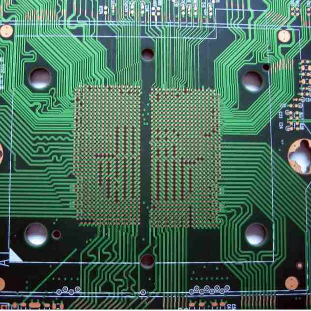
What are blind vias?
Blind vias, also known as buried vias, are holes that connect different layers of a printed circuit board (PCB) without being visible or accessible from the surface of the board. The via is plated through, allowing electric currents to flow between layers, but the ends are covered by copper so they cannot be probed or accessed.
Blind vias are most commonly used for:
- Connecting layers in multilayer boards
- Avoiding interference, crosstalk or shorting between layers
- Reducing manufacturing costs by eliminating through-hole drilling
Benefits of using blind vias
Using blind vias offers several advantages compared to through-hole vias:
More routing space
With blind vias, the entire surface of the PCB can be used for routing traces since there are no visible via holes that need to be avoided. This allows for more efficient use of the board space.
Lower costs
Blind vias only require drilling between the layers they connect, not the entire thickness of the board. This reduces drilling time and materials, lowering manufacturing costs.
Higher density
The lack of surface holes allows blind vias to be placed closer together, enabling higher via and trace density. More components and connections can be fit into the same space.
Reduced EMI
Fully shielded blind vias emit less electromagnetic interference (EMI) compared to through-hole vias, which act as antennas. This helps meet EMI and FCC requirements.
Layer isolation
Blind vias prevent unwanted contacts between layers, reducing electrical shorts and crosstalk. Signals can be contained within layers.
Improved impedance control
With no drilled hole, blind vias allow for more consistent impedance across a PCB layer, improving high-speed signals.
Easier probing
No holes means fewer obstacles when probing the PCB surface during testing.
Higher strength
The uninterrupted board surface provides greater mechanical strength and durability.
When should blind vias be used?
Blind vias are ideal in many situations, but a few key uses cases include:
- High density, complex PCBs such as phones and handheld devices
- Multilayer boards with 4 layers or more
- High frequency analog or digital boards
- Boards requiring controlled impedance for signals
- Low cost consumer electronics with tight space requirements
Here are a few examples of where blind vias may be preferable to through-hole vias:
Cell phones
The compact layout of cell phone PCBs makes drilling through-hole vias difficult. Blind vias allow connections between layers without disrupting the densely packed surface components.
Automotive electronics
The multilayer boards in cars need to withstand vibration and thermal stresses. Blind vias provide mechanical strength while electrically interconnecting layers.
IoT devices
Miniature IoT products need small, reliable PCBs. Blind vias enable more compact layouts and prevent shorting between layers.
High speed digital logic
To maintain signal integrity at high frequencies, blind vias give better impedance control than through-hole vias.
RF boards
Onboards RF components, contained signals and consistent impedance are crucial. Blind vias prevent interference between layers.
Challenges of working with blind vias
While blind vias provide many benefits, they also impose some design restrictions:
- Only adjacent layers can be connected, not non-adjacent layers. Additional vias may be required.
- Blind vias cannot be probed or visually inspected from the surface.
- Impedance matching is critical to avoid signal reflection at the via.
- Blind and buried vias require more complex PCB fabrication processes.
- Repairing blind vias is very difficult or impossible. The entire board may need replacing.
- Blind via failures can be hard to diagnose since they are not accessible.
To mitigate these challenges:
- Use stackup planning tools to optimize layer arrangements and via placements
- Build impedance matching into board and via design
- Ensure manufacturers validate full via connectivity and layer bonding
- Implement thorough post-manufacture testing and inspection processes
- Consider using filled or tented vias for easier repair and rework
Best practices for working with blind vias
Here are some top tips for effectively utilizing blind vias:
Carefully plan layer stackup
Map out board layer arrangement and sequence to minimize necessary blind depths. Place critical high-speed traces near the stackup center if possible.
Follow fabrication guidelines
Work within recommended aspect ratios for minimum hole size/spacing and maximum depth. This avoids reliability issues.
Maintain impedance
Match blind via barrel impedance to that of traces, typically 50-100 ohms. Use impedance calculators to determine ideal via dimensions.
Allow for fabrication tolerances
Design blind vias slightly larger than specified to account for hole misregistration, layer misalignment, etc.
Add test points
Since blind vias can’t be probed, include strategically placed test points to validate connectivity.
Perform thorough testing
Execute complete board functional testing to uncover any potential blind via defects that visual inspection would miss.
Use blind/buried vias judiciously
Limit use only to applications where they provide significant benefit. Avoid complicating the board design unnecessarily.
Consult manufacturer recommendations
Seek guidance from fabricators on best practices for your specific board technology and processes.
Example stackups using blind vias
Here are two common PCB layer stackup configurations using blind vias, illustrating why they are useful:
6-layer board with blind vias
| Layer | Function |
|---|---|
| 1 (top) | Component side |
| 2 | Ground plane |
| 3 | Signal 1 |
| 4 | Power plane |
| 5 | Signal 2 |
| 6 | Ground plane |
| 7 (bottom) | Solder side |
- Blind vias connect layers 2-3, 3-5, and 5-7 without penetrating power plane
- Provides isolation between signal layers and uninterrupted power distribution
- Allows high density component placement on surface
10-layer board with blind and buried vias
| Layer | Function |
|---|---|
| 1 (top) | Component side |
| 2 | Ground |
| 3 | Signal 1 |
| 4 | Power 1 |
| 5 | Signal 2 |
| 6 | Signal 3 |
| 7 | Ground |
| 8 | Signal 4 |
| 9 | Power 2 |
| 10 | Solder side |
- Blind vias connect layers 2-3, 5-8
- Buried vias connect layers 4-6
- Provides 5 routing layers with power/ground separation
- High speed signals isolated on inner layers
Alternative via types
While blind vias provide many advantages, other via types may be more suitable for some applications:
Through-hole vias
Simple and inexpensive, but disrupt board surface routing and emit EMI.
Tented vias
Partially covered blind vias allow rework and repair. Impede some routing.
Filled vias
Blind vias filled with epoxy. Reduce emission loss but increase cost.
Buried vias
No connection to outer layers. Used to route internal inner layers only.
Microvias
Small vias (~0.2mm) allow very high density. Require advanced processes.
Staggered vias
Use several smaller offset vias for thermal management and impedance control.
The ideal via type depends on density, manufacturability, thermal needs, isolatation, impedance, and other specific design requirements.
Summary
To recap, key points about blind vias:
- Blind vias connect PCB layers without penetrating the entire board
- They optimize routing space, lower costs, and improve performance
- Blind vias isolate signals, prevent interference, and enable high-density PCBs
- Use is limited to adjacent layers, requiring more vias for more layers
- Impedance control and thorough testing is crucial with blind vias
- Blind vias should be designed conservatively to account for tolerances
- They provide significant benefits but involve more complex fabrication
For multilayer boards with high density or high frequency requirements, the advantages of using blind vias typically outweigh the additional considerations required in design and manufacturing. As PCBs become more complex and performance-driven, blind and buried vias will continue gaining traction over traditional through-hole vias.
FAQ
Here are answers to some frequently asked questions about blind vias:
What are some typical blind via sizes?
Blind via sizes commonly range from 0.2 mm to 0.5 mm in diameter depending on the PCB technology. High density boards may use microvias as small as 0.1 mm.
What is the maximum aspect ratio for blind vias?
The aspect ratio (height/diameter) should generally not exceed 8:1. Ratios above 10:1 often result in unreliable plating.
Are there recommended pad sizes for blind vias?
Pads are usually 1.2 to 2 times larger than the blind via diameter. For a 0.3 mm via, a 0.6 mm pad allows for tolerances.
How do you calculate impedance for a blind via?
Use a blind via impedance calculator based on dimensions, barrel material, drilling angles, and desired impedance (usually 50-100Ω).
Can buried and blind vias be combined on one PCB?
Yes, blind vias connect adjacent layers while buried vias route only internal layers. A board may use both via types.


Leave a Reply