Why is Soldermask Thickness Important?
The thickness of the soldermask layer is a critical factor in PCB design and manufacturing for several reasons:
-
Insulation: Soldermask acts as an insulating layer, preventing unwanted electrical connections between copper traces. The thickness of the soldermask directly affects its insulating properties.
-
Protection: Soldermask protects the copper traces from oxidation, corrosion, and mechanical damage during handling and assembly. A thicker soldermask layer provides better protection.
-
Solder Control: The thickness of the soldermask influences how well it controls the flow of molten solder during the soldering process. A proper thickness ensures that solder only adheres to the exposed pads and does not bridge between traces.
-
Impedance Control: In high-frequency PCBs, the soldermask thickness can affect the impedance of the transmission lines. Consistent and controlled soldermask thickness is essential for maintaining the desired impedance.
Standard Soldermask Thicknesses
Soldermask thickness is typically measured in mils (thousandths of an inch) or microns (μm). The most common soldermask thicknesses used in the PCB industry are:
| Thickness (mils) | Thickness (μm) | Application |
|---|---|---|
| 0.5 – 0.8 | 12.7 – 20.3 | Standard PCBs |
| 1.0 – 1.2 | 25.4 – 30.5 | High-reliability PCBs |
| 1.5 – 2.0 | 38.1 – 50.8 | Extreme environments |
The choice of soldermask thickness depends on the specific requirements of the PCB, such as the operating environment, the level of protection needed, and the desired electrical properties.
Impact on Insulation and Protection
Insulation Resistance
Insulation resistance (IR) is a measure of the soldermask’s ability to prevent current from flowing between adjacent conductors. A higher IR value indicates better insulation properties. The thickness of the soldermask directly affects its insulation resistance.
As a general rule, increasing the soldermask thickness improves its insulation properties. However, there is a point of diminishing returns, where further increases in thickness do not significantly improve insulation resistance. The table below shows the relationship between soldermask thickness and insulation resistance:
| Thickness (mils) | Insulation Resistance (MΩ) |
|---|---|
| 0.5 | 500 |
| 0.8 | 1,000 |
| 1.0 | 1,500 |
| 1.2 | 2,000 |
It is essential to choose a soldermask thickness that provides sufficient insulation resistance for the specific application while considering other factors such as cost and manufacturability.
Protection Against Environmental Factors
Soldermask also serves as a protective layer, shielding the copper traces from environmental factors such as moisture, chemicals, and mechanical stress. A thicker soldermask layer generally offers better protection against these factors.
For example, in harsh industrial environments where PCBs may be exposed to corrosive chemicals or high humidity, a thicker soldermask (1.5 – 2.0 mils) is often used to provide enhanced protection. In less demanding environments, a standard thickness (0.5 – 0.8 mils) may be sufficient.

Impact on Solder Control
Soldermask thickness plays a crucial role in controlling the flow of molten solder during the soldering process. If the soldermask is too thin, it may not effectively prevent solder bridging between closely spaced pads or traces. On the other hand, if the soldermask is too thick, it can hinder the formation of proper solder joints.
The ideal soldermask thickness for solder control depends on several factors, including:
- Pad and Trace Spacing: Closely spaced pads and traces require a thicker soldermask to prevent bridging.
- Solder Paste Thickness: The thickness of the applied solder paste should be considered when choosing the soldermask thickness to ensure proper solder joint formation.
- Soldering Method: Different soldering methods (e.g., wave soldering, reflow soldering) may have different requirements for soldermask thickness.
The table below provides general guidelines for selecting soldermask thickness based on pad and trace spacing:
| Pad/Trace Spacing (mils) | Recommended Soldermask Thickness (mils) |
|---|---|
| > 20 | 0.5 – 0.8 |
| 10 – 20 | 0.8 – 1.0 |
| < 10 | 1.0 – 1.2 |
It is essential to work closely with the PCB manufacturer and assembly house to determine the optimal soldermask thickness for a specific design and manufacturing process.
Impact on Impedance Control
In high-frequency PCBs, such as those used in radio frequency (RF) and high-speed digital applications, the soldermask thickness can affect the impedance of the transmission lines. Impedance control is critical in these applications to ensure signal integrity and minimize reflections and distortions.
The dielectric constant (Dk) of the soldermask material and its thickness contribute to the overall dielectric constant of the PCB stackup. Variations in soldermask thickness can lead to impedance mismatches and signal integrity issues.
To maintain consistent impedance, it is essential to control the soldermask thickness tightly. PCB manufacturers use specialized equipment and processes to apply soldermask with high precision and uniformity. Some common methods for controlling soldermask thickness include:
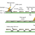
- Screen Printing: A stencil is used to apply soldermask to the PCB surface. The thickness is controlled by the stencil thickness and the printing parameters.
- Curtain Coating: Soldermask is applied as a continuous curtain, and the thickness is controlled by the speed of the conveyor and the viscosity of the soldermask material.
- Spray Coating: Soldermask is sprayed onto the PCB surface, and the thickness is controlled by the spray parameters and the number of coats applied.
For high-frequency PCBs, it is common to specify a soldermask thickness tolerance of ±0.1 mils (±2.5 μm) to ensure consistent impedance across the board.
Soldermask Thickness Measurement
Accurate measurement of soldermask thickness is essential for quality control and ensuring that the PCB meets the specified requirements. There are several methods for measuring soldermask thickness, including:
- Cross-Sectional Analysis: A small section of the PCB is cut and polished, and the soldermask thickness is measured using a microscope.
- Micrometer: A micrometer is used to measure the thickness of the PCB before and after soldermask application. The difference between the two measurements is the soldermask thickness.
- Eddy Current Testing: A non-destructive method that uses electromagnetic induction to measure the thickness of non-conductive coatings on conductive substrates.
- Ultrasonic Testing: A non-destructive method that uses high-frequency sound waves to measure the thickness of the soldermask layer.
PCB manufacturers typically use a combination of these methods to ensure that the soldermask thickness meets the specified tolerances.
FAQ
-
What is soldermask, and why is it essential in PCB manufacturing?
Soldermask is a thin layer of polymer applied to the copper traces of a PCB. It serves as an insulating and protective layer, preventing solder bridging and protecting the copper from oxidation and mechanical damage. Soldermask is essential for ensuring the reliability and performance of PCBs. -
How does soldermask thickness affect the insulation properties of a PCB?
The thickness of the soldermask directly affects its insulation resistance. A thicker soldermask layer generally provides better insulation between adjacent conductors. However, there is a point of diminishing returns, where further increases in thickness do not significantly improve insulation resistance. -
What is the recommended soldermask thickness for high-frequency PCBs?
For high-frequency PCBs, it is essential to control the soldermask thickness tightly to maintain consistent impedance. A common soldermask thickness tolerance for high-frequency PCBs is ±0.1 mils (±2.5 μm). The specific thickness depends on the PCB stackup and the desired impedance. -
How is soldermask thickness measured?
There are several methods for measuring soldermask thickness, including cross-sectional analysis, micrometer measurement, eddy current testing, and ultrasonic testing. PCB manufacturers typically use a combination of these methods to ensure that the soldermask thickness meets the specified tolerances. -
Can soldermask thickness be customized for specific applications?
Yes, soldermask thickness can be customized based on the specific requirements of the PCB. Factors such as the operating environment, the level of protection needed, and the desired electrical properties influence the choice of soldermask thickness. It is essential to work closely with the PCB manufacturer to determine the optimal thickness for a specific application.
Conclusion
Soldermask thickness is a critical factor in PCB design and manufacturing, impacting insulation, protection, solder control, and impedance control. Choosing the appropriate soldermask thickness depends on the specific requirements of the PCB, such as the operating environment, the level of protection needed, and the desired electrical properties.
PCB manufacturers use specialized equipment and processes to apply soldermask with high precision and uniformity, ensuring consistent thickness across the board. Accurate measurement of soldermask thickness is essential for quality control and meeting specified tolerances.
By understanding the impact of soldermask thickness on PCB performance and working closely with PCB manufacturers, designers can ensure that their boards meet the required specifications and perform reliably in their intended applications.

Leave a Reply