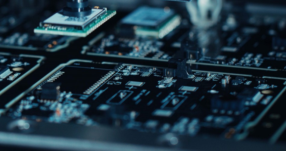
Printed circuit boards (PCBs) are an essential component of most electronic devices. They provide the platform for mounting and connecting electronic components using conductive tracks and pads. The manufacture of PCBs involves many processes, each requiring specialized machinery. This article explores the major PCB manufacturing machines involved from start to finish.
1. Design and Layout
The first step in manufacturing PCBs is designing the board layout. This is done using CAD (computer-aided design) software that allows the designer to lay out the circuit board’s components, routing, layer stackup and more. Popular PCB design software includes:
1.1. Altium Designer
One of the leading PCB design tools, Altium Designer provides a full suite of capabilities for schematic capture, PCB layout/routing, 3D modeling and library management. It generates manufacturing output files like Gerber, NC drill, assembly drawings and more.
1.2. Cadence Allegro
Allegro by Cadence Design Systems offers high-end PCB layout and routing features. It is widely used for complex, multi-layer boards and provides integration with MCAD tools.
1.3. Mentor Graphics Xpedition
Xpedition is a comprehensive electronics design platform by Mentor Graphics with PCB/IC packaging design, simulation, analysis and manufacturing release capabilities.
1.4. Zuken CR-8000
The CR-8000 from Zuken is used widely in the automotive, telecom and industrial electronics industries. It has an intuitive layout interface and integrates with MCAD for enclosures.
2. Imaging and Photoplotting
Once the PCB layout is designed, the next step is transferring the design onto the copper-clad laminate. Photoplotting machines are used for imaging the PCB patterns onto film that will be used to etch copper selectively. The key equipment here includes:
2.1. Imagesetters
Imagesetters use laser direct imaging (LDI) technology to image the PCB patterns directly from CAD data onto photo-resist coated boards. They image inner and outer layers separately with high precision down to under 10 microns. Popular imagesetters are from companies like Orbotech, Limata and others.
2.2. Plotters
Plotters are used to print PCB layout patterns onto transparent film or paper. They typically have resolutions between 500 DPI to 2540 DPI. Liquid-ink, thermal transfer and toner-based electrostatic plotters are commonly used. Leading vendors include HP, OCE, Xerox, etc.
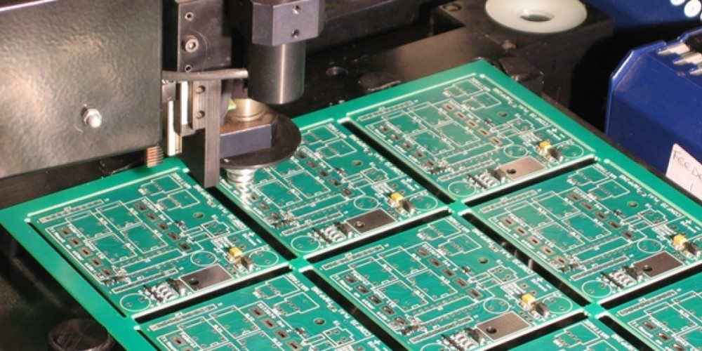
3. Etching Processes
Etching is the process of selectively removing copper from the PCB laminate to leave only the desired conductive pattern on the board. The primary etching machinery includes:
3.1. Laminators
Laminators are used to combine the photoresist coated copper boards with the imaged films, aligning them accurately. This transfers the pattern onto the photoresist coating. Common laminating processes are roller, heat and vacuum pressure lamination.
3.2. Developers
After lamination, the boards undergo developing where they are exposed to a chemical solution that dissolves the unexposed photoresist to uncover the unwanted copper. Typical developers use spray or immersion processes.
3.3. Etchers
Etching removes the uncovered copper selectively to leave behind only the conductive pattern masked by photoresist. Etchers use chemical solutions like ferric chloride or cupric chloride under controlled temperature and agitation. Batch processing spray and conveyorized etchers are commonly used.
3.4. Strippers
Strippers remove the remaining photoresist mask from the PCBs after etching, revealing the finished copper circuits. They typically use alkaline solutions or solvents.
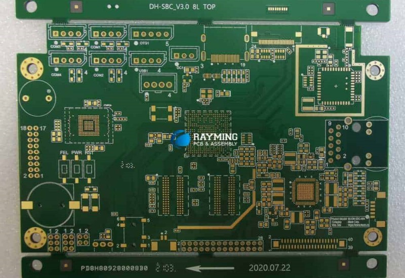
4. Drilling Processes
PCBs require hundreds or thousands of holes to mount electronic components. Highly specialized drilling machines are essential in PCB fabrication.
4.1. Mechanical Drills
Mechanical drilling units use carbide drill bits for making through-hole vias and holes up to 1 mm diameter. They have high speed spindles reaching over 90,000 RPM and X-Y tables for precise positioning.
4.2. CNC Drills
CNC drilling machines have multiple drilling spindles and automated X-Y positioning systems. They are programmable to drill panels of multiple PCBs efficiently. Leading CNC drill makers include Excellon, Hitachi, Pluritec, etc.
4.3. Laser Drills
Laser drilling systems use pulsed uv lasers focused through lenses to ablate material and make microvias. They drill holes down to 0.002” with high precision and no tool wear or breakage issues.
5. Surface Finishing
The fabricated PCBs undergo a number of finishing processes and treatments using specialized equipment:
5.1. Brushers/Scrubbers
These machines use rotating brushes/abrasives to clean the PCBs of debris and processing residues. They ensure good adhesion for subsequent plating processes.
5.2. Electroless Copper Deposition
This step chemically deposits a thin copper layer onto the drilled hole walls and surfaces to make them conductive prior to electroplating. Wet chemical processing tanks are used.
5.3. Electrolytic Plating
Electrolytic plating units use copper/tin/lead anodes to deposit metal finish layers like copper, tin-lead, nickel-gold etc. onto PCBs giving them solderability and protection.
5.4. Spray Washers
PCBs are washed after various chemical processes using high pressure spray washers or immersion tanks that thoroughly clean off etching, plating and drilling residues.
5.5. Hot Air Solder Levelling
HASL machines deposit a solder coating on PCBs to facilitate component soldering. The PCBs pass through molten solder then air knives to leave a thin solder layer.
6. Electrical Testing
Testing machines are essential for quality assurance and identifying any shorts, opens or errors in fabricated boards:
6.1. Flying Probe Testers
These have movable test probes for contacting test points on a panel of PCBs and rapidly perform continuity/isolation testing.
6.2. ICT Fixtures
ICT test fixtures with bed-of-nails or pogo pins make contact with test pads on assembled boards for in-circuit testing to verify proper connections.
6.3. AOI Systems
Automated optical inspection machines check bare PCBs and assembled boards using cameras to identify defects like spurious copper, missing holes/features, wrong components etc.
7. Assembly and Packaging
Additional machines are used by PCB assembly houses to populate the boards with components and finish them:
7.1. Pick and Place
Robotic pick-and-place systems precisely place tiny surface mount devices onto PCBs at very high speeds using miniaturized vacuum nozzles.
7.2. Reflow Ovens
SMT components are soldered using reflow ovens that systematically heat the PCBs to melt the solder paste deposited during placement.
7.3. Wave Soldering
Through-hole components are soldered on a moving PCB using a molten wave of solder. Board washers clean off flux residues after soldering.
7.4. Conformal Coating
A protective polymer coating is sprayed onto finished PCB assemblies using automated selective coating machines or robots.
7.5. Lead Forming/Cutting/Crimping
Axial component leads are trimmed, formed and crimped using high speed belt-fed machines before placement on boards.
This covers some of the major types of machines used throughout the PCB manufacturing and assembly process. The variety of equipment reflects the complexity of reliably producing quality printed circuit boards. With newer additive processes on the horizon, the machinery ecosystem will continue evolving alongside PCB technology itself. Proper selection and maintenance of these machines is key to achieving efficient, high-yield and consistent production.
Frequently Asked Questions
Q1. What are the main steps in PCB manufacturing?
The main steps in PCB manufacturing are:
- Design and layout
- Imaging/Photoplotting
- Etching
- Drilling
- Surface finishing
- Electrical testing
- Assembly
Each step involves specialized machinery like photoplotters, etchers, drills, plating equipment, pick-and-place, etc.
Q2. What is the most critical machine in PCB fabrication?
The most critical machines in PCB fabrication are the photoplotters and etchers. The photoplotters transfer the PCB layout onto the boards while the etchers selectively remove copper to produce the desired circuit pattern. Defects in these processes can ruin entire PCB panel runs.
Q3. How are holes drilled in PCBs?
Holes are drilled in PCBs using computerized numerical control (CNC) drilling machines and laser drilling machines. CNC drills use high speed carbide bits for standard through-hole drilling while lasers make microvias. The drilling accuracy and precision determines PCB quality.
Q4. What machines are used for PCB prototyping?
Some common machines used in PCB prototyping are:
- Small-format photoplotters for imaging
- Compact wet chemical or dry film photoresist etching tools
- Benchtop drilling machines
- Manual plating tanks
- Tabletop AOI and testers
This allows developing a few PCB prototypes without investing in full-scale manufacturing equipment.
Q5. How are components assembled on PCBs?
Component assembly machines for PCBs include:
- Pick-and-place machines to accurately place tiny SMT devices
- Reflow ovens to solder SMT parts
- Wave soldering systems for through-hole components
- Conformal coating applicators for protection
- Lead trimming/forming machines
The assembly steps demand high precision automation to achieve quality and reliability.
In summary, PCB manufacturing involves a wide variety of machinery spanning design, imaging, material removal and additive processes, cleaning, inspection and assembly. The capabilities of this equipment ultimately determines the complexity, density and quality achievable in the PCB fabrication process. Careful selection and maintenance is key to building an efficient PCB production line.


Leave a Reply