Introduction
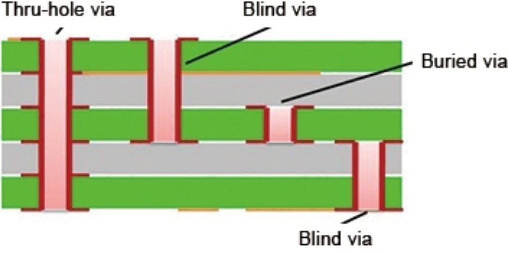
A blind via is a hole that connects different layers of a printed circuit board (PCB) together electrically without having a pad on the external layers. Blind vias are often used to route connections between inner layers of a multilayer PCB while keeping the outer surfaces free of vias for components and traces. The size of a blind via depends on various factors like current carrying capacity, drill bit sizes, and fabrication capabilities. This article provides a detailed overview of blind via sizes, their measurement, influencing factors, and industry standards.
Standard Sizes of Blind Vias
IPC Standards for Blind Via Sizes
The IPC or The Institute for Interconnecting and Packaging Electronic Circuits sets industry standards for PCBs, including blind via sizes. According to IPC-2221A standards, the finished hole size of blind vias can range from 0.25 mm to 0.75 mm. The typical drill sizes to achieve these finished hole sizes are:
| Drill Size | Finished Hole Size |
|---|---|
| 0.2 mm | 0.25 mm |
| 0.3 mm | 0.35 mm |
| 0.4 mm | 0.45 mm |
| 0.5 mm | 0.55 mm |
| 0.6 mm | 0.65 mm |
| 0.7 mm | 0.75 mm |
So a 0.3 mm drill is used for a 0.35 mm finished blind via as per IPC guidelines. The industry standard hole size is 0.35 mm.
Typical Aspect Ratios
The aspect ratio refers to the ratio of the thickness of the PCB to the drill diameter of the blind via. A via with a higher aspect ratio is more challenging to produce. The IPC-2221A recommends maximum aspect ratios of 8:1 to 10:1 for blind vias.
For a 1.6 mm thick PCB, common blind via sizes would be:
- 0.2 mm drill (8:1 aspect ratio)
- 0.3 mm drill (5.3:1 aspect ratio)
- 0.4 mm drill (4:1 aspect ratio)
Minimum Annular Rings
The annular ring is the pad area surrounding the blind via. IPC guidelines recommend minimum annular rings of 0.15 mm to 0.2 mm for blind vias. So for a 0.3mm finished blind via, the pad size would need to be around 0.7 mm to 0.8 mm including the annular ring.
Factors Affecting Blind Via Sizing

The size of a blind via hole and finished diameter depends on various PCB design considerations:
Number of layers
More number of layers means blind vias connect more layers together. For 6-8 layer boards, 0.2mm to 0.3mm drill sizes are common. For high-density interconnect boards with 20+ layers, drill sizes are usually under 0.15mm.
Current carrying capacity
Larger hole sizes allow more current handling capacity. For power circuits above 1A current, 0.4mm or larger blind vias are preferred.
PCB thickness
Thicker boards need larger aspect ratio vias. For boards above 3.2mm thickness, 0.3mm or larger drills are typical.
Routing density
Denser designs require many small vias. High speed digital PCBs often use 0.2mm or 0.15mm microvias.
Manufacturing capabilities
The minimum hole size the PCB manufacturer can reliably produce affects blind via sizing. Laser drilling can achieve microvias down to 0.1mm.
Cost
Smaller blind vias require specialized drilling equipment and advanced processes which increases fabrication costs. Larger vias are cheaper to manufacture.
Blind Via Size Calculation
The IPC-2221A provides equations to calculate the finished hole size based on drill diameter:
- For drill diameters below 0.35 mm:
- Finished Hole Size = Drill Diameter + 0.10 mm
- For drill diameters above 0.35 mm:
- Finished Hole Size = Drill Diameter + 0.15 mm
So for a 0.2 mm drill, the finished hole size would be 0.2 + 0.1 = 0.25 mm.
And for a 0.5 mm drill, the finished hole size would be 0.5 + 0.15 = 0.65 mm.
Blind Via Size Selection Guidelines
Here are some best practices for selecting appropriate blind via sizes in PCB design:
- Use larger vias for high current power circuits. Aim for 0.4 mm or 0.5 mm finished hole size.
- For digital circuits, 0.2 mm or 0.3 mm vias can suffice depending on routing density.
- Ensure aspect ratio is within 8:1 to 10:1 limits as per IPC guidelines.
- Leave adequate annular ring of 0.15mm to 0.2mm around the pad.
- Consider manufacturer’s capabilities. Consult with your PCB fabricator on their minimum via capability.
- Weigh costs vs performance. Smaller vias impact fabrication costs and yields.
- Use via in pad design where possible to maximize routing space.
- Employ proper via spacing rule of thumb: Distance between vias should be ≥ 2 x hole size.
By selecting the optimal blind via size, you can achieve reliable inter-layer connections while minimizing manufacturing issues like opens or shorts.
Typical Blind Via Applications

Here are some common applications for blind vias in PCBs:
Connecting surface mount pads to inner layers
Blind vias can connect IC pads to power or ground planes internally without occupying space on the surface.
Fan-out escape routing
Blind/buried vias allow routing signals from densely packed BGAs or other components to less congested inner layers.
RF/high speed design
Strategic use of blind/buried vias can provide impedance matching and controlled impedance routing for high frequency circuits.
Mixed signal routing
Sensitive analog signals can be routed on inner layers separately from noisy digital signals on outer layers using blind/buried vias.
High density interconnects
HDI PCBs with microvias help achieve compact routing for complex ICs with pin counts over 500.
3D/multilayer packaging
Blind vias enable vertical systemic integration by connecting multiple PCBs stacked together.
Blind Via Manufacturing Processes
There are several techniques used to produce blind vias during PCB fabrication:
Laser Drilling
A laser beam is used to sequentially drill through the layers required to form a blind via. Allows very small microvias down to 0.10 mm.
Photo VIA
A laser is used to expose a sensitised dielectric layer to create vias. Allows 0.15mm microvia with thin dielectric buildup.
Plasma Etching
Plasma gas removes dielectric material to selectively form blind vias. Best for high density boards over 20 layers.
CNC Drilling
Computer numerical control (CNC) mechanical drilling can produce blind vias by controlling drill depth precisely. Cost effective, minimum size 0.20mm.
The manufacturing process capabilities determine the smallest attainable blind via size. Reliable production yields are also a key consideration during fabrication.
Comparison of Blind, Buried and Through-Hole Vias
| Parameter | Blind Via | Buried Via | Through-Hole Via |
|---|---|---|---|
| Connects | Between outer layer and one or more inner layers | Between two or more inner layers only | All layers from top to bottom |
| Requires pad on outer layers | No | No | Yes |
| Drilling method | Sequential laser or plasma | Sequential laser or plasma | Single mechanical drill through |
| Current capacity | Medium | Medium | Highest |
| Cost | Medium | Highest | Lowest |
| Routing density | High | Highest | Low |
| EMI shielding | Poor | Best | Good |
Key Differences:
- Blind vias offer higher routing density than through-hole but less than completely buried vias.
- Blind vias provide no EMI shielding unlike buried vias between layers.
- Blind and buried vias cost more than drilled through-hole vias.
FAQ
What are the typical sizes for microvias in HDI PCBs?
For high density interconnect (HDI) PCBs, microvias down to 0.15 mm drilled diameter are common. This results in 0.18-0.2mm finished blind via holes.
What is the optimal spacing between blind vias?
As a rule of thumb, the clearance between blind vias should be at least 2 times the via hole size. This prevents drilling quality and plating issues.
Can blind vias be stacked?
Yes, blind vias can be stacked vertically if required for routing density. But keep their centers aligned to prevent reliability issues like opens/shorts.
How close can a blind via be to a surface mount pad?
It is recommended to keep 0.5mm clearance between a blind/buried via and an SMT pad for better soldering quality.
How are blind vias filled during fabrication?
Blind vias are either tenting filled with epoxy or plugged filled with electrolytic or electroless copper plating. Plugged fills offer the best heat dissipation.


Leave a Reply