Introduction
When designing printed circuit boards (PCBs), engineers must choose between different technologies for creating conductive pathways and mounting components. Two of the most common options are high-density interconnect (HDI) and through hole technology. While both technologies have their place in PCB design, they differ significantly in their characteristics and applications.
This article will examine the key differences between HDI and through hole technology. We will look at how each one works, their respective advantages and disadvantages, and when to use one versus the other. Understanding these distinctions allows engineers to select the best technology for their particular PCB design needs.
How HDI Works
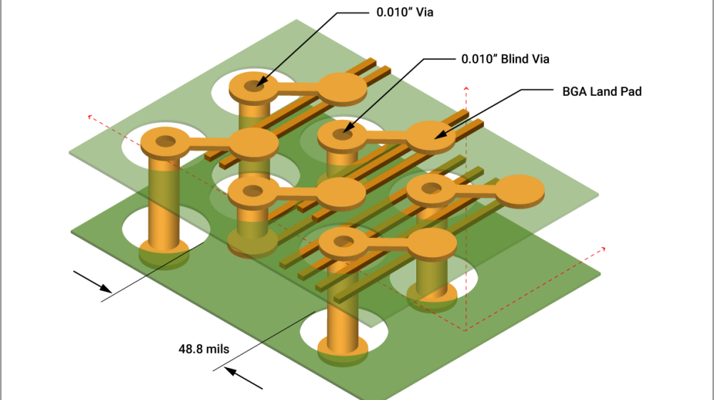
HDI refers to technology that allows for incredibly dense interconnections on a PCB. It enables trace lines and spaces under 6 mils wide, versus 8-10 mils for standard PCBs.
HDI accomplishes this via a layered approach. First, fine lines and spaces are fabricated on the inner layers of the PCB. Then, these layers are stacked together and laminated. Laser drilling forms microvias to interconnect the layers. These microvias have a diameter of around 0.005 inches or less. Finally, outer conventional circuitry completes the board.
In this manner, HDI allows four to sixteen circuit layers or more. This equates to high component density, accommodating advanced miniaturized devices. The layers involved in HDI include:
- HDI dielectric layers – Thin insulating dielectric material, such as polyimide. This enables fine trace widths and close spacing.
- HDI circuit layers – Thin copper layers with laser defined traces and spaces less than 6 mils.
- Blind vias – Holes laser drilled only through a portion of the HDI stackup to make layer-to-layer connections.
- Buried vias – Blind vias that do not reach either the top or bottom of the board.
- Microvias – Small vias with diameters less than 6 mils drilled with a laser.
- Staggered microvias – Offset microvias to connect to various buried layers.
- Skip vias – Microvias that skip adjacent layers to connect non-adjacent layers.
This complex structure allows routing dense interconnects both vertically and horizontally within the PCB stackup.
Advantages of HDI
Here are some of the major advantages of using HDI technology:
- High density – The main appeal of HDI is the incredibly dense circuitry it facilitates. HDI allows packing more interconnects into a smaller PCB footprint.
- Miniaturization – The fine features of HDI permit further miniaturization of PCBs and associated electronic devices. This facilitates applications like smartphones, wearables, and Internet of Things nodes.
- High-speed – Thin dielectrics and close conductor spacing means lower capacitance. This allows faster signal propagation for high-speed applications.
- Reliability – HDI processes utilize advanced materials that can withstand higher temperatures. This improves thermal cycling reliability.
- Design flexibility – The layered approach provides more routing options, allowing for greater design freedom. Complex routing can be achieved.
- Embedded components – Active and passive components can be embedded within the HDI layers to save space.
Disadvantages of HDI
The advanced nature of HDI technology does introduce some downsides:
- Expense – HDI PCBs cost significantly more to manufacture than conventional boards. Both the materials and fabrication processes involved are pricey.
- Limited Fab access – Only advanced PCB fabricators have the capability to produce HDI boards. This could restrict sourcing options.
- Design complexity – HDI requires more complex and constrained layer stackup decisions during layout. This makes PCB design more difficult.
- Testability issues – It can be harder to test and inspect the buried traces and microvias within an HDI board non-destructively.
- Repairability issues – Similarly, troubleshooting faults and performing rework on HDI boards also poses challenges.
- Fragility – The thin dielectrics and conductors are more prone to damage during handling. Care must be taken.
How Through Hole Technology Works
The term “through hole technology” refers to the traditional approach of using drilled holes to mount components and make interconnections in a PCB. These holes pass fully through the circuit board from top to bottom.
In terms of circuit board fabrication, through holes are made with mechanical drilling. The most common drill bit diameters range from 0.3mm to 3mm. For component holes, finished sizes range from 0.4mm to 2.5mm or more.
Through hole technology connections involve:
- PTHs (plated-through holes) – Holes used to route signals vertically across layers are plated with copper. This forms a continuous conductive pathway via electroplating.
- Component leads – Leaded components are inserted through holes drilled at appropriate spacing. Solder joins the leads.
- Vias – Plated-through holes interconnect layers without inserting components.
- Pads – Annular copper pads surround holes to facilitate soldering.
- Jumper wires – Small gauge insulated wires can be used to manually wire jumper connections on boards.
This type of PCB fabrication and component assembly represents a mature, well-established process. It has been widely used since the 1950s.
Advantages of Through Hole Technology
Below are some of the advantages offered by the through hole approach:
- Mature technology – Through hole fabrication is extremely well understood with a very wide experience base. It is considered highly reliable.
- Compatible components – Many leaded components are readily available at low cost for through hole boards.
- Easy visual inspection – Through hole solder joints are visible for easy inspection. Board failure points can often be diagnosed by looking at the PCB.
- Easy troubleshooting – Similarly, components on through hole boards can be easily probed or replaced for troubleshooting. Jumper wires can modify circuits.
- Good for harsh conditions – The large through hole solder joints withstand shock, vibration, and thermal cycling well.
- Easy manual assembly – Through hole components can be hand soldered without specialized tools. Hand assembly remains viable.
- Low cost – Overall, through hole PCB fabrication and component costs are very inexpensive compared to other technologies. This makes it ideal for high volume cost-sensitive products.
Disadvantages of Through Hole Technology
Some weaknesses of the through hole approach include:
- Larger components – Leaded through hole components take up a lot more space than surface mount devices. This limits miniaturization.
- Lower component density – The through hole assembly process limits how many components can be packed onto a PCB. Component crowding becomes an issue.
- Limited I/O density – Similarly, lower trace densities throttle interconnect capacity. Complex high I/O devices often cannot be supported.
- No blind/buried vias – All vertical connections occupy board real estate since they must run between top and bottom layers.
- No embedded components – Only surface mounted components are an option. No embedding components within the board itself.
- Lower speeds – Through hole boards generally only support slower digital signals below 25 MHz clocks. High speed analog is also challenging.
- Not reworkable – Removing and replacing leaded components once soldered tends to damage pads and lifts traces. Rework is very difficult.
- Only one-sided SMT – Some SMT parts can be used, but only on one side. The plated through holes occupy space on the opposite side.
Comparisons Between HDI and Through Hole
Below we summarize some of the major differences between the HDI and through hole PCB technologies:
| Parameter | HDI | Through Hole |
|---|---|---|
| Line width/spacing | Under 6 mil | 8 mil minimum |
| Via diameter | Microvias under 6 mil | 0.4 – 2.5mm or larger holes |
| Layers | Up to 20+ | Typically only 2-8 layers |
| Traces | Very dense routing | Limited trace density |
| Components | Mainly surface mount | Mix of through hole and SMT |
| Design | Complex stackup/layout | Simpler layout |
| Speeds | Multi-GHz possible | Under 25MHz typically |
| Currents | Lower max current | Handles higher currents |
| Cost | Very expensive | Low cost boards |
| Volume | Medium to high quantity | All quantities |
This comparison shows that HDI is positioned at the cutting edge of dense, high-speed PCBs. It enables sophisticated designs not otherwise possible. In contrast, through hole technology offers a basic, low cost PCB fabrication option well suited for simple, high volume boards.
When to Use Each Technology
In general, here are some guidelines on when to use each PCB technology:
Applications for HDI
- High density interconnections
- Miniature and portable products
- High speed computing like servers
- Advanced consumer devices
- Cutting edge aerospace/defense
- Next generation telecom infrastructure
Applications for Through Hole
- High reliability, harsh environments
- Very high volume cost-sensitive goods
- Legacy products with existing libraries
- Education and hobbyists
- Rapid prototyping and testing
Of course, the choice depends on the specific requirements of the application. Many designs utilize both HDI and through hole technology on different areas of the same PCB. However, in general HDI suits advanced applications requiring miniaturization and performance, while through hole serves basic high volume applications where simplicity and cost are king.
Conclusion
This examination of HDI and through hole technologies clarifies the very different roles they serve in PCB design. HDI enables dense routing and layers to meet the interconnect demands of modern electronics. It paves the way for continued miniaturization and innovation. However, through hole retains advantages in reliability, ease of assembly, and low cost. This sustains its dominance for high quantity mass-produced boards without advanced requirements.
Understanding this divergence helps engineers select the right PCB technology for their needs during the design process. HDI and through hole each have their place, and often complement each other on different areas of the same board. With a grasp of the comparative strengths and weaknesses, engineers can employ each one where it makes the most sense. This knowledge helps strike the optimal balance of sophistication, performance and cost when laying out printed circuit boards.
Frequently Asked Questions
Q: What are the key differences between HDI and through hole PCB technology?
A: The main differences are:
- HDI enables much denser trace lines and spaces (less than 6 mil) versus 8 mil minimum for through hole.
- HDI utilizes microvias under 6 mil diameter versus 0.4 – 2.5mm holes for through hole.
- HDI supports many more layers (20+) versus 2-8 for through hole.
- HDI accommodates primarily SMT components versus through hole’s mix of SMT and leaded components.
- HDI permits much higher speeds and densities versus slower, simpler through hole boards.
Q: What are the main advantages of HDI and through hole respectively?
A:
HDI advantages:
- Very high density routing
- Facilitates miniaturization
- High speed signal propagation
- Improved thermal cycling reliability
- More routing flexibility
Through hole advantages:
- Mature, well-understood technology
- Compatible with many leaded components
- Easy visual inspection and debugging
- Withstands harsh mechanical environments
- Lower overall fabrication costs
Q: When should I use HDI versus through hole?
A: In general:
Use HDI for:
- Cutting edge consumer devices
- Compact, high performance designs
- Next generation aerospace/defense
- High density interconnections
Use Through hole for:
- Very high volume, cost-sensitive goods
- Simple, legacy products
- Education and hobbyists
- Rapid prototyping
Q: Can HDI and through hole be used together on the same PCB?
A: Yes, many designs use HDI technology in the dense areas of the board that require it. Less complex areas can utilize through hole components and routing where cost is more important than space. The technologies complement each other.
Q: What are some of the main disadvantages or limitations of HDI?
A: Disadvantages of HDI include:
- Much higher fabrication costs
- More complex design constraints
- Potential rework and repair difficulties
- Fragile nature of thin dielectrics/conductors
- Requires advanced PCB fabricators


Leave a Reply