Introduction
HDI (High Density Interconnect) and PCB (Printed Circuit Board) are two important technologies used in the electronics industry for building circuits and components. Both play a crucial role in circuit design and manufacturing. However, there are some key differences between the two that designers and engineers need to understand.
In this article, we will compare HDI and PCB in detail, looking at what they are, their construction, their use cases and applications, and the main differences between the two technologies.
What is HDI?
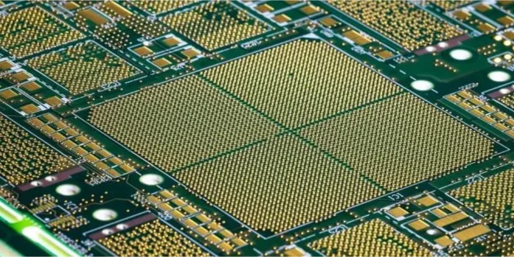
HDI stands for High Density Interconnect. As the name suggests, HDI refers to printed circuit boards (PCB) that have a higher wiring density than conventional PCBs.
HDI PCBs enable finer lines and spaces, smaller vias, and higher connection pad densities compared to standard PCBs. This is achieved through advanced PCB fabrication processes that allow for thinner dielectric layers and more closely spaced traces.
Some key characteristics of HDI PCBs:
- Trace width and spacing of 5 mils or less
- Microvias with diameters of 6 mils or less
- Thinner dielectric material layers (1 mil or less)
- More circuit layers (up to 20 layers or more)
- Higher wiring density
- Fine line traces and spaces
HDI technology was developed to meet the needs of shrinking component sizes and rising interconnectivity demands in advanced electronics. Cell phones, wearables, Internet of Things (IoT) devices, automotive electronics, and other compact but complex electronic products rely on HDI PCBs.
HDI Construction
There are a few key construction differences that distinguish HDI PCBs from standard PCBs:
- Layer Stackup: HDI PCBs have a layer stackup optimized for higher wiring density. This includes thinner dielectric layers separating close conductor layers.
- Trace Width/Spacing: HDI PCBs have much finer trace widths and tighter trace spacing, down to 5 mils or less. This increases wiring density.
- Microvias: HDI PCBs use microvias with very small diameters (6 mils or under) to allow more connections between layers.
- High Density Interconnects: HDI PCBs have dense connections and high interconnectivity between layers to maximize routing in the small space.
- Landless Vias: HDI PCBs can use landless or capless vias where the via goes directly from one trace layer to the next without connecting pads, further increasing density.
- Laser Drilling: Microvias are often drilled with laser drills to achieve the precision needed for small via diameters.
What is PCB?
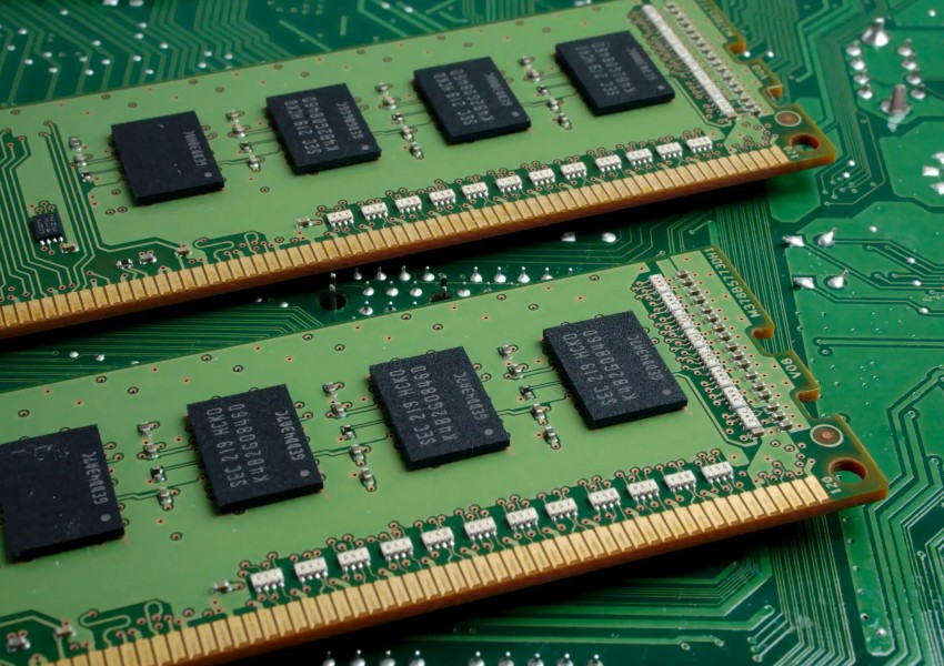
PCB stands for Printed Circuit Board. This is the generic term used for boards designed to support and connect electronic components using conductive pathways or traces etched from copper sheets and laminated onto a non-conductive substrate.
PCBs provide the mechanical structure to mount and electronically connect components using etched copper traces and pads. They are the platform that powers most electronics we use.
PCB Construction
Standard PCB construction involves:
- Substrate layers made from insulating materials like FR-4 fiberglass.
- Copper foil layers that are patterned using etching to form the conductive traces, pads, and connections.
- Alternating layers of substrate and patterned copper foils stacked up and laminated together under heat and pressure.
- Drilled holes called vias that interconnect the conductor layers.
- Finished with solder mask and silkscreen layer for protection and component markings.
PCBs can have anywhere from a single layer to over 20 layers depending on the circuit complexity. Multilayer boards allow more interconnections between components.
Key Differences Between HDI and PCBs
While HDI PCBs are a type of PCB, there are some important differences between HDI and standard PCBs:
| Parameter | HDI PCB | Standard PCB |
|---|---|---|
| Dielectric Layer Thickness | 1 mil or less | Typically 2 to 4 mils |
| Trace Width/Spacing | 5 mils or smaller | 8 mils or greater |
| Microvia Diameter | 6 mils or under | Typically 8 to 10 mils |
| Routing Density | Very High | Moderate |
| Layer Count | Up to 20+ | Typically 4-8 layers |
| Construction | Optimized for density | Not optimized for density |
| Drilling | Uses laser drilling | Traditional mechanical drilling |
| Cost | More expensive | Lower cost |
Key Differences Summary:
- Thinner Dielectric Layers: HDI PCBs use thinner insulating dielectric layers between copper layers, allowing closer trace spacing.
- Narrower Traces and Spaces: HDI PCBs achieve finer trace widths and tighter trace spacing.
- Smaller Microvias: Microvias on HDI PCBs have smaller diameters, enabling greater interconnect density.
- Higher Routing Density: HDI PCBs maximize routing and interconnect density.
- More Layers: HDI designs utilize more circuit layers with dense vertical connections.
- Laser Drilling: HDI microvias are often laser drilled for precision and density.
- Higher Cost: HDI PCBs cost more due to advanced materials and processes.
HDI PCB Applications and Use Cases
The high wiring density and interconnectivity of HDI PCBs make them ideal for advanced circuits and compact electronics applications where routing space is at a premium.
Some common applications and use cases for HDI PCB technology include:
- Smartphones: HDI allows the dense circuitry required to fit inside thin smartphones.
- Wearable Devices: HDI provides the interconnect density needed for small wearables.
- Internet of Things (IoT): Interconnecting many components in small IoT devices requires HDI.
- Automotive Electronics: Advanced driver assistance systems and infotainment rely on HDI.
- RF/Wireless Devices: HDI supports integrated antennas and high frequency analog circuits.
- Medical Devices: Implants and compact medical electronics leverage HDI technology.
- Military/Aerospace: Avionics, guidance systems, and other space-constrained defense electronics benefit from HDI.
In contrast, standard PCB technology is suitable for many consumer, industrial, and commercial electronics where ultra-high density interconnect is not required.
PCB Applications and Use Cases
Since PCBs encompass everything from simple single-sided boards to multilayer boards, they have an extremely broad range of applications across many industries and products including:
- Consumer electronics – game consoles, TVs, home appliances
- Computers – motherboards, graphics cards, storage devices
- Automotive – engine control units, infotainment, body electronics
- Communications – routers, switches, base stations
- Industrial automation and control systems
- Medical equipment
- Military/aerospace/avionics systems
- IoT connected devices
- Test and measurement equipment
- And many more!
Almost every electronic device uses one or more PCBs to interconnect and support the components that enable its functionality. Standard PCB technology still powers a wide range of electronic products and systems that do not require the advanced capabilities of HDI PCBs.
Advantages and Disadvantages of HDI vs. PCBs

HDI PCB Advantages:
- Enables greater routing density and component miniaturization.
- Allows for more compact and thinner end products.
- Supports integration of more functions and components.
- Allows higher speed signals and circuit performance.
- Enables advanced circuits for cutting edge applications.
HDI PCB Disadvantages:
- Significantly higher fabrication costs due to advanced processes.
- Requires specialized design expertise and training.
- Process control and standards are still maturing.
- More prone to defects and lower yields.
- Often has large minimum order quantities.
Standard PCB Advantages:
- Well-established, reliable and cost-effective fabrication.
- Easier design rules and processes.
- Sufficient for many applications without complexity of HDI.
- Mature industry standards and supply chain.
Standard PCB Disadvantages:
- Limited in routing density and interconnects.
- Not suitable for advanced miniaturized devices.
- Cannot support leading-edge chip technologies.
- Less capable at high speeds and RF applications.
By understanding the pros and cons of each technology, engineers can select the right PCB platform for their product requirements. HDI provides maximum density and integration capabilities for advanced devices, while standard PCBs offer proven performance for mainstream applications.
Conclusion and Summary
In summary, while HDI PCB and standard PCB technologies share common aspects in their construction and fabrication, there are distinct differences:
- HDI PCBs prioritize maximizing interconnect density, trace width/spacing, microvia dimensions and routing channels.
- Standard PCBs do not require the same level of density and optimization.
- HDI PCBs enable smaller, higher performance advanced electronics used in smartphones, IoT devices, wearables, automotive, aerospace, and medical applications.
- Standard PCBs continue to serve most electronics involving simpler or larger assemblies across consumer, industrial, and other commercial applications.
Engineers weigh factors like cost, technical needs, product constraints, and production volume when determining whether HDI or standard PCB technology is the right fit for an electronics design and manufacturing project.
Frequently Asked Questions (FAQ)
Here are some common questions about HDI PCBs and how they compare to standard PCBs:
Q: What are the typical trace widths and spacings on an HDI PCB?
A: HDI PCBs commonly have trace widths and spacings of 5 mils (0.127mm) or smaller. Standard PCB trace widths are typically 8 mils or greater.
Q: Why are dielectric layers thinner in HDI PCBs compared to standard PCBs?
A: Thinner dielectric layers in HDI PCBs allow bringing the conductive layers closer together. This enables higher trace density and more layers in a given thickness.
Q: What are some key benefits of using microvias in HDI PCBs?
A: Microvias provide more interconnects between layers in a smaller space. This facilitates routing dense connections in HDI designs.
Q: What size products typically use HDI PCB technology?
A: HDI PCBs are predominantly used in smaller, compact electronics like smartphones, wearables, and Internet of Things (IoT) devices where space is extremely limited.
Q: Are HDI PCBs more prone to manufacturing defects compared to standard PCBs?
A: Yes, the dense small features in HDI PCBs make them more prone to physical defects and lower yields, which also drives their higher costs.


Leave a Reply