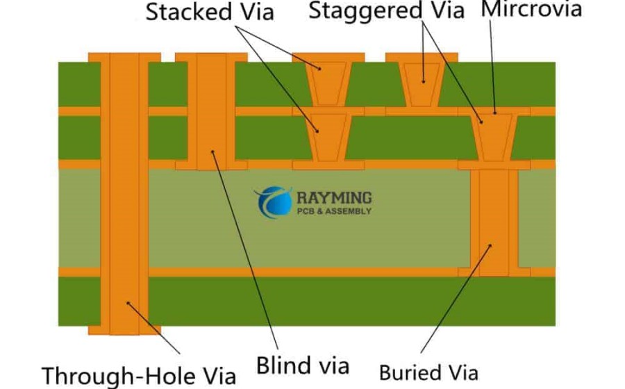
Introduction to microvias and their various types
The continuous miniaturization of electronics has led to shrinking component sizes and PCB features. As a result, the via structure, which provides the electrical interconnect between the various layers of a printed circuit board (PCB), has also evolved over the years. Some of the key developments in via structures include:
- Standard through-hole via: A plated through hole that connects two or more layers in a PCB while also allowing component leads to pass through. These are the traditional via structures.
- Blind via: A plated through hole that connects two or more layers but does not go through the entire PCB stackup.
- Buried via: A plated through hole that connects internal layers only, without connecting to the outer layers.
The continued reduction in feature sizes led to the development of an even smaller via structure called the microvia. Microvias have diameters smaller than 150 microns (or 0.15 mm). Based on their structure and usage, microvias can be classified into three main types:
- Via-in-pad (VIP): A microvia that is formed within a surface mount pad, allowing interconnection between layers without using space on the surface layer.
- Stacked microvia: Multiple vias stacked vertically to form a continuous interconnect between layers. This helps minimize surface area usage.
- Staggered microvia: Microvias arranged in a staggered manner through multiple layers for reliability and improved interconnect density.
What is a via-in-PAD (VIP)?
A via-in-pad (VIP) is a type of microvia that is constructed within the surface mount pads on the PCB. As the name suggests, instead of placing the via and pad separately, a VIP incorporates the via within the surface mount pad area.
Some key characteristics of VIPs:
- VIPs have a typical diameter between 80-150 microns.
- They are formed within the SMD copper pad area, thus saving significant real estate.
- VIPs occupy the complete thickness of the PCB, interconnecting all layers.
- Laser or photolithography processes are typically used for drilling microvias.
- VIPs allow for higher interconnect density and more routing channels.
- They can accommodate pitches down to 0.3mm, enabling compact layouts.
- VIPs improve electrical performance by providing low inductance/resistance paths.
- Reliability is enhanced as there are no traces routed between closely spaced pads.
By incorporating the microvia within the pad structure, VIPs eliminate the need to route traces between adjacent SMD pads for layer-to-layer interconnections. This allows more routing channels on the board layers along with space savings on the surface finish. VIPs are commonly used in designs that require high-density footprints like BGAs, CSPs, 01005 passives, etc. They enable miniaturization for applications in consumer electronics, aerospace, automotive, and medical devices.
What is a Microvia?
Microvias, as the name indicates, are just smaller-sized vias typically with a diameter less than 150um (0.15mm). They were developed to meet the ever-increasing demands for greater interconnect densities in printed circuit boards.
Here are some typical characteristics of microvias:
- Diameters range from 50um to 150um, compared to 300um and above for conventional vias
- Aspect ratios (height:diameter) up to 10:1
- Allow routing traces with width and spacing down to 100um
- High density arrangements with pad pitches up to 0.3mm
- Provides more routing channels on inner layers
- Optimized for surface mount components like 0402 passives and CSPs
- Improved electrical performance at higher frequencies
- Fabricated using laser ablation or photolithography processes
- Require appropriate stackup materials to avoid reliability issues
Microvias enable dense vertical interconnects that were not feasible with conventional plated through-hole vias. They are an essential enabling technology for HDI (High Density Interconnect) PCBs used widely in consumer electronics, military systems, medical devices, etc. VIPs are a specialized type of microvia tailored for high I/O component pads.
Key Differences between VIPs and Microvias
While VIPs and microvias share the same drilling processes and dimensional attributes, there are some key differences in their structure and usage:
| Parameter | Via-in-PAD (VIP) | Microvia |
|---|---|---|
| Location | Constructed within surface mount pads | Can be placed anywhere on PCB including non-pad areas |
| Pad Size | Same as component pad size, no additional pads | May require separate pads on each layer for reliable interconnection |
| Routing | No traces routed between adjacent pads | Traces can be routed between pads & vias |
| Layers Connected | Typically interconnect all layers | Can selectively connect between layers |
| Land Pattern | Defined by component pad | Additional land pattern may be required |
| Design Rules | Contained within pad area | Space must be allocated during layout |
| Applications | Dense packages like BGAs, CSPs | Interconnects in standard and HDI designs |
Some key points regarding the differences:
- Location: VIPs save space by utilizing the SMD pad area while microvias can be placed anywhere with adequate spacing.
- Pad Size: VIPs do not need separate pads as they use the existing SMD copper pad. Microvias may require additional pads on each layer for a reliable connection.
- Routing: No traces can be routed between VIP pads. But routing is allowed between microvias and pads.
- Layers: VIPs typically interconnect all layers from the outer pad. Microvias can selectively connect between layers as per layout requirements.
- Land Pattern: VIP pad size is defined by the component footprint. Microvias may need additional pads/land patterns.
- Design Rules: VIPs only impact the pad area. Microvias require additional board space for placement.
- Applications: VIPs are optimal for dense footprints while microvias serve more general interconnection requirements.
Fabrication and Reliability Considerations
Fabricating PCBs with microvias and VIPs require several considerations from the material and process perspectives to ensure reliable performance under thermal and mechanical stresses:
- Thin dielectric layers (around 50um) with low CTE (coefficient of thermal expansion) like polyimide
- Stackup with low overall Z-axis CTE to minimize warpage and stresses
- Surface finishes with direct plating like ENEPIG or ENIG are preferred
- Laser microvia drilling techniques provide high precision
- Pad size, microvia barrels, and capture pads must be optimized
- Plating thickness should be adequate for current loads without reliability risks
- Sufficient annular ring size must be maintained around drilled vias
- Regular hole wall metallization helps anchor connections
- Appropriate lamination pressure, temperature profiles, and drill smear removal techniques should be applied
- Electrical testing, cross-section analysis, and thermal stress testing helps validate reliability
With the right stackup, material selection, layout strategies, and fabrication processes, microvias and VIPs can reliably deliver the interconnect performance and densities needed in advanced PCB designs.
Frequently Asked Questions
Q1. What are the key benefits of using VIPs and microvias?
The major benefits of using VIPs and microvias include:
- Increased routing channels from space savings
- Higher interconnect densities
- Miniaturization and optimal footprint for advanced packages
- Improved electrical performance at high frequencies
- Elimination of stubs for better signal integrity
- Lower power distribution impedances
- Overall technology enablement for thinner and smaller designs
Q2. What are the typical production challenges with microvias?
Some typical production challenges with microvias that require close attention are:
- Achieving consistent hole wall metallization for reliable connections
- Optimizing fabrication process parameters like lamination pressure, temperature, and ramp rates
- Precise drilling and controlling via barrel profiles
- Reliably plating small blind and buried microvias
- Having adequate capture pads sizes to accommodate tolerances
- Eliminating drill smear and debris after drilling
- Minimizing weepage of plating chemistry into dielectric
- Avoiding overplating or underplating defects
- Effectively testing interconnect continuity for buried microvias
- Validating assembly and reliability performance
Q3. How are VIPs and microvias formed in the PCB fabrication process?
VIPs and microvias are formed using the following typical steps:
- Drilling using laser ablation or photolithographic techniques
- Desmear to remove debris after drilling
- Metallization using direct plating or panel plating processes
- Electrolytic copper plating to build up barrel thickness
- Plating resist application and patterning to define circuitry
- Surface finish plating – typically ENEPIG or ENIG
- Plating resist stripping
- Panel lamination using appropriate materials
- Drilling larger holes/vias if required
- Final Cu patterning and etching to form pads, traces etc.
- Solder mask coating and patterning
- Final PCB routing into individual boards
Q4. What are some best practices to incorporate VIPs/microvias in the PCB design phase?
Some VIP/microvia design best practices include:
- Minimize unsupported span of pads over VIPs/microvias
- Include thermal relief connections for large copper pours
- Allow adequate pullback from pad edges for tolerances
- Use teardrop pads on inner layers for better anchorages
- Do not place microvias at board outline locations
- Maintain minimum annular ring of around 25um whenever possible
- Reduce pad size if VIPs are over 30% of area to prevent cracking
- Plan finished hole size, barrel profile, and capture pads appropriately
- Densely space VIPs/microvias for better lamination stability
- Check aspect ratio limits based on stackup construction
Q5. How is reliability testing performed for microvias and VIPs?
Typical qualification and reliability testing approaches for microvias include:
- IST (interconnect stress test) – thermal cycles combined with board flexing
- HAST (highly accelerated stress test) – temperature, humidity, bias conditions
- Drop/shock testing – assess mechanical robustness
- Vibration testing – examine connection integrity under vibratory loads
- Solder reflow simulation – validate process compatibility
- Cross-section analysis – inspect interface connections and barrel profiles
- Four-point probing – check for electrical opens after exposures
- Optical inspection – evaluate plating defects or cracks
- Impedance testing – match high-speed channel characteristics


Leave a Reply