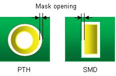
What is a Solder Mask?
Before diving into Solder mask dam, it’s crucial to understand what a solder mask is. A solder mask is a thin layer of polymer that is applied to the surface of a PCB. Its primary purpose is to protect the copper traces and pads from oxidation, prevent solder bridges from forming between adjacent pads, and provide electrical insulation. Solder masks also serve as a barrier against environmental factors such as moisture, dust, and debris.
Solder masks are typically green in color, but they can also be found in other colors such as red, blue, yellow, and black. The choice of color depends on the specific requirements of the PCB and the preferences of the manufacturer or client.
| Property | Description |
|---|---|
| Material | Polymer (epoxy, acrylic, or polyimide) |
| Thickness | 0.0005 to 0.002 inches (0.0127 to 0.0508 mm) |
| Color | Green (most common), red, blue, yellow, black |
| Purpose | Protection, insulation, and solder control |
What is a Solder Mask Dam?
A solder mask dam is a raised feature on a PCB that is created by selectively applying a thicker layer of solder mask between two adjacent pads or traces. The purpose of a solder mask dam is to prevent solder from flowing between these pads or traces during the soldering process. By controlling the flow of solder, solder mask dams help maintain the integrity of the electrical connections and prevent short circuits.
Solder mask dams are particularly useful in high-density PCB designs where the spacing between pads and traces is minimal. They are also essential in applications where the PCB is subjected to harsh environmental conditions or mechanical stress, as they provide additional protection against solder bridging and other defects.

How Does a Solder Mask Dam Work?
The working principle of a solder mask dam is based on the surface tension of molten solder. When solder is heated during the assembly process, it becomes liquid and tends to flow towards areas of lower surface tension. By creating a physical barrier (the solder mask dam) between two adjacent pads or traces, the surface tension of the molten solder is disrupted, preventing it from flowing across the dam.
The effectiveness of a solder mask dam depends on several factors, including:
-
Dam height: The height of the solder mask dam should be sufficient to prevent solder from flowing over it. A typical dam height ranges from 0.1 to 0.15 mm.
-
Dam width: The width of the solder mask dam should be designed to accommodate the specific requirements of the PCB. A wider dam provides better protection but may also increase the overall size of the PCB.
-
Solder mask material: The choice of solder mask material can affect the performance of the solder mask dam. Some materials, such as liquid photoimageable (LPI) solder masks, offer better resolution and adhesion compared to traditional dry film solder masks.
-
Solder type and volume: The type and volume of solder used during the assembly process can also influence the effectiveness of the solder mask dam. It’s essential to consider these factors when designing the dam to ensure optimal performance.

Applications of Solder Mask Dams
Solder mask dams find applications in various industries where PCBs are used, including:
-
Consumer electronics: Smartphones, tablets, laptops, and other consumer electronic devices often feature high-density PCB designs that require solder mask dams to ensure reliable connections and prevent short circuits.
-
Automotive: PCBs used in automotive applications are subjected to harsh environmental conditions, such as extreme temperatures, vibrations, and moisture. Solder mask dams provide additional protection against solder bridging and other defects that could compromise the functionality and safety of the vehicle.
-
Medical devices: PCBs used in medical devices must meet stringent reliability and performance standards. Solder mask dams help ensure the integrity of the electrical connections, reducing the risk of device failure and patient harm.
-
Aerospace and defense: PCBs used in aerospace and defense applications often require high levels of reliability and durability. Solder mask dams provide an extra layer of protection against solder bridging and other defects that could compromise the performance of the equipment.
-
Industrial automation: PCBs used in industrial automation systems are exposed to harsh environmental conditions and mechanical stress. Solder mask dams help maintain the integrity of the electrical connections, ensuring the reliable operation of the equipment.

Frequently Asked Questions (FAQ)
-
Q: Can solder mask dams be used on both sides of a PCB?
A: Yes, solder mask dams can be applied to both sides of a PCB, depending on the specific design requirements. -
Q: How are solder mask dams created?
A: Solder mask dams are created by selectively applying a thicker layer of solder mask between two adjacent pads or traces during the PCB manufacturing process. This is typically done using photolithography techniques. -
Q: Can solder mask dams be used with any type of solder?
A: Solder mask dams can be used with most types of solder, including lead-based and lead-free solder. However, it’s essential to consider the specific properties of the solder when designing the dam to ensure optimal performance. -
Q: Are there any limitations to using solder mask dams?
A: While solder mask dams provide an effective solution for controlling solder flow, they may not be suitable for all PCB designs. In some cases, the added thickness of the solder mask dam may increase the overall size of the PCB or affect its mechanical properties. -
Q: How can I ensure the effectiveness of solder mask dams in my PCB design?
A: To ensure the effectiveness of solder mask dams, it’s essential to consider factors such as dam height, width, solder mask material, and solder type and volume. It’s also recommended to work closely with your PCB manufacturer to optimize the design and ensure the best possible results.
Conclusion
Solder mask dam is a critical feature in PCB design that helps control the flow of solder during the assembly process. By creating a physical barrier between adjacent pads or traces, solder mask dams prevent solder bridging and ensure the reliability and functionality of the final product. With applications in various industries, from consumer electronics to aerospace and defense, solder mask dams play a vital role in ensuring the quality and performance of PCBs.
As PCB designs continue to become more complex and high-density, the importance of solder mask dams will only continue to grow. By understanding the principles behind solder mask dams and how they work, PCB designers and manufacturers can create more reliable and efficient products that meet the demands of today’s rapidly evolving technologies.


Leave a Reply