How Peelable Soldermask Works
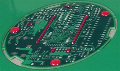
The peelable soldermask is a polymer-based material that is applied to the PCB surface in liquid form, typically through screen printing or spray coating. Once applied, the soldermask is cured using heat or ultraviolet (UV) light, forming a solid, protective layer over the desired areas of the PCB.
The key feature of peelable soldermask is its ability to be easily removed after the soldering process is complete. This is achieved through the use of specially formulated polymers that have a lower adhesion to the PCB surface compared to traditional permanent soldermasks.
Advantages of Using Peelable Soldermask
-
Selective soldering: Peelable soldermask allows for precise control over which areas of the PCB are exposed to solder. This is particularly useful for components that require specific soldering techniques or when different components need to be soldered at different times.
-
Protection from solder bridging: By covering the areas between pads and traces, peelable soldermask helps prevent solder bridging, which can cause short circuits and other issues.
-
Cost-effective: Compared to other methods of selective soldering, such as using permanent soldermask with multiple openings or employing expensive selective soldering machines, peelable soldermask offers a more affordable solution.
-
Improved efficiency: Peelable soldermask streamlines the PCB assembly process by reducing the need for multiple soldering steps and minimizing the risk of errors.
Applications of Peelable Soldermask
Peelable soldermask finds applications across various industries and PCB types, including:
-
High-density PCBs: As electronic devices become smaller and more complex, high-density PCBs with closely spaced components are becoming increasingly common. Peelable soldermask enables precise soldering of these components without the risk of solder bridging.
-
Double-sided PCBs: When assembling double-sided PCBs, peelable soldermask can be used to protect the components on one side while soldering the other side.
-
Rework and repair: Peelable soldermask is useful for PCB rework and repair, as it allows technicians to access specific components without damaging the surrounding areas.
-
Prototype development: In the prototype stage, peelable soldermask enables quick and easy modifications to the PCB layout without the need for expensive and time-consuming permanent soldermask changes.
Peelable Soldermask Application Process
The application of peelable soldermask involves several steps:
-
PCB preparation: The PCB surface is cleaned and dried to ensure proper adhesion of the soldermask.
-
Soldermask application: The peelable soldermask is applied to the PCB using screen printing or spray coating, covering the desired areas.
-
Curing: The soldermask is cured using heat or UV light, depending on the specific product used.
-
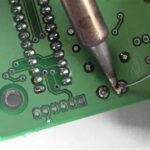
Soldering: The exposed areas of the PCB are soldered, while the areas covered by the peelable soldermask remain protected.
-
Soldermask removal: After soldering, the peelable soldermask is carefully removed, leaving a clean PCB surface with precisely soldered components.
| Step | Process | Purpose |
|---|---|---|
| 1 | PCB preparation | Ensures proper adhesion of soldermask |
| 2 | Soldermask application | Covers desired areas with peelable soldermask |
| 3 | Curing | Solidifies the soldermask using heat or UV light |
| 4 | Soldering | Solders exposed areas while protecting covered areas |
| 5 | Soldermask removal | Removes the peelable soldermask, leaving a clean PCB |

Choosing the Right Peelable Soldermask
When selecting a peelable soldermask for your PCB assembly process, consider the following factors:
-
Compatibility with PCB materials: Ensure that the peelable soldermask is compatible with the PCB substrate material and any other coatings or finishes used.
-
Curing method: Choose a soldermask that cures using a method compatible with your manufacturing process, such as heat or UV light.
-
Removal ease: Consider the ease of removal for the soldermask, as some products may require specific techniques or solvents for clean and efficient removal.
-
Temperature resistance: If your soldering process involves high temperatures, select a peelable soldermask with an appropriate temperature resistance rating.
-
Environmental impact: Opt for peelable soldermasks with low volatile organic compound (VOC) content and minimal environmental impact.
Troubleshooting Peelable Soldermask Issues
While peelable soldermask offers numerous benefits, some common issues may arise during use:
-
Incomplete removal: If the soldermask is not completely removed after soldering, it can interfere with subsequent assembly steps or affect the PCB’s final appearance. To avoid this, ensure that the soldermask is properly cured and use the appropriate removal technique.
-
Residue on PCB surface: In some cases, peelable soldermask may leave residue on the PCB surface after removal. This can be minimized by selecting a high-quality soldermask and following the manufacturer’s recommended removal process.
-
Inadequate protection: If the peelable soldermask is not applied properly or does not adhere well to the PCB surface, it may not provide adequate protection during soldering. Ensure that the PCB surface is clean and dry before applying the soldermask and follow the manufacturer’s application guidelines.
Future Developments in Peelable Soldermask Technology
As the demand for advanced PCB assembly techniques grows, peelable soldermask technology continues to evolve. Some potential future developments include:
-
Improved environmental sustainability: Manufacturers are working on developing peelable soldermasks with even lower VOC content and reduced environmental impact.
-
Enhanced temperature resistance: As soldering temperatures continue to rise, new peelable soldermask formulations with higher temperature resistance will be needed.
-
Faster curing and removal times: To further streamline the PCB assembly process, manufacturers are focusing on developing peelable soldermasks that cure and can be removed more quickly.
-
Integration with automated assembly processes: As PCB assembly becomes increasingly automated, peelable soldermask application and removal processes will need to be adapted to work seamlessly with robotic systems.
Frequently Asked Questions (FAQ)
-
Q: Can peelable soldermask be used on both rigid and flexible PCBs?
A: Yes, peelable soldermask can be used on both rigid and flexible PCBs, provided that the specific product is compatible with the PCB substrate material. -
Q: How long does it take for peelable soldermask to cure?
A: The curing time for peelable soldermask depends on the specific product and the curing method used (heat or UV light). Typically, curing times range from a few minutes to an hour. -
Q: Is peelable soldermask reusable?
A: No, peelable soldermask is designed for single use and must be removed and discarded after the soldering process is complete. -
Q: Can peelable soldermask be used for wave soldering?
A: Yes, peelable soldermask can be used for wave soldering, providing protection for specific areas of the PCB during the soldering process. -
Q: Are there any special storage requirements for peelable soldermask?
A: Peelable soldermask should be stored in a cool, dry place, away from direct sunlight and heat sources. Always refer to the manufacturer’s storage guidelines for specific requirements.
In conclusion, peelable soldermask is a valuable tool in the PCB assembly process, offering selective soldering capabilities, cost-effectiveness, and improved efficiency. As PCB designs become more complex and the demand for advanced assembly techniques grows, peelable soldermask technology will continue to evolve to meet the needs of the industry.
Leave a Reply