Introduction to PCB Visualizer
PCB Visualizer is a powerful software tool designed to help engineers, designers, and manufacturers create, analyze, and optimize printed circuit board (PCB) designs. It provides a comprehensive set of features that enable users to visualize, simulate, and troubleshoot PCB layouts, ensuring high-quality and reliable electronic products. With its intuitive interface and advanced capabilities, PCB Visualizer has become an essential tool in the electronics industry.
Key Features of PCB Visualizer
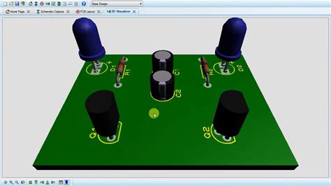
- 3D Visualization
- Realistic 3D rendering of PCB designs
- Interactive exploration of components and layers
-
Ability to rotate, zoom, and pan the 3D model
-
Real-time Design Rule Checking (DRC)
- Automatic detection of design rule violations
- Customizable design rule settings
-
Instant feedback for error correction
-
Signal Integrity Analysis
- Simulation of signal integrity issues
- Identification of crosstalk, reflections, and other anomalies
-
Recommendations for improving signal quality
-
Thermal Analysis
- Simulation of heat distribution on the PCB
- Identification of hot spots and thermal bottlenecks
-
Optimization of component placement for better heat dissipation
-
Component Library Management
- Extensive library of electronic components
- Ability to create and customize component models
- Integration with popular CAD tools
Benefits of Using PCB Visualizer
PCB Visualizer offers numerous benefits to engineers, designers, and manufacturers in the electronics industry. Some of the key advantages include:
- Improved Design Quality
- Early detection and correction of design flaws
- Optimization of component placement and routing
-
Reduction of errors and rework
-
Enhanced Collaboration
- Sharing of 3D models and design data
- Facilitation of cross-functional communication
-
Streamlined design review and approval processes
-
Time and Cost Savings
- Faster design iterations and prototyping
- Reduction of physical prototypes and testing
-
Shorter time-to-market for electronic products
-
Increased Reliability
- Identification and mitigation of potential failure points
- Improvement of signal integrity and thermal performance
- Higher quality and longevity of electronic devices
Getting Started with PCB Visualizer
System Requirements
To run PCB Visualizer effectively, your computer should meet the following minimum system requirements:
| Component | Minimum Requirement |
|---|---|
| Operating System | Windows 10, macOS 10.14, or Linux (Ubuntu 18.04) |
| Processor | Intel Core i5 or equivalent |
| RAM | 8 GB |
| Graphics Card | Dedicated GPU with 2 GB VRAM |
| Storage | 500 GB HDD or 256 GB SSD |
Installation Process
Installing PCB Visualizer is a straightforward process. Follow these steps to get started:
- Download the PCB Visualizer installer from the official website.
- Double-click the installer file to begin the installation process.
- Follow the on-screen instructions, accepting the license agreement and choosing the installation directory.
- Select the desired components and features to install.
- Click “Install” to start the installation.
- Once the installation is complete, launch PCB Visualizer from the desktop shortcut or the Start menu.
User Interface Overview
PCB Visualizer offers a user-friendly interface that allows you to navigate and interact with your PCB designs easily. The main window is divided into several sections:
- Toolbar
- Contains commonly used tools and functions
- Includes options for opening, saving, and exporting designs
-
Provides access to visualization settings and analysis tools
-
3D View
- Displays the 3D rendering of the PCB design
- Allows interaction with the model, such as rotation, zooming, and panning
-
Enables the selection and manipulation of components and layers
-
Properties Panel
- Shows detailed information about selected components or nets
- Allows editing of component properties and parameters
-
Provides access to design rule settings and constraints
-
Layer Manager
- Lists all the layers in the PCB design
- Allows enabling or disabling the visibility of specific layers
-
Provides options for layer stacking and ordering
-
Output Window
- Displays messages, warnings, and errors generated during design analysis
- Shows the results of simulations and calculations
- Provides feedback on design rule violations and suggested fixes

Working with PCB Designs
Creating a New PCB Design
To create a new PCB design in PCB Visualizer, follow these steps:
- Click “File” in the toolbar and select “New” from the dropdown menu.
- Choose the desired PCB template or start with a blank design.
- Set the board dimensions, layer stack-up, and other initial properties.
- Click “OK” to create the new PCB design.
Importing Existing Designs
If you have an existing PCB design created in another CAD tool, you can easily import it into PCB Visualizer:
- Click “File” in the toolbar and select “Import” from the dropdown menu.
- Choose the file format of your existing design (e.g., Gerber, ODB++, IPC-2581).
- Browse and select the design file from your computer.
- Click “Open” to import the design into PCB Visualizer.
Adding and Placing Components
To add components to your PCB design, follow these steps:
- Open the component library by clicking “Library” in the toolbar.
- Search for the desired component using keywords or categories.
- Drag and drop the component onto the PCB design surface.
- Position the component by clicking and dragging it to the desired location.
- Rotate or flip the component if necessary using the context menu or keyboard shortcuts.
Routing and Connecting Traces
PCB Visualizer provides powerful tools for routing and connecting traces between components:
- Select the “Route” tool from the toolbar.
- Click on the starting pad or via of the trace.
- Move the cursor to the desired endpoint and click to place the trace segment.
- Continue clicking to add additional segments or press “Esc” to finish the trace.
- Adjust the trace width, layer, and other properties using the Properties panel.
Running Design Rule Checks
To ensure your PCB design meets the required specifications and constraints, PCB Visualizer offers automated design rule checking (DRC):
- Click “Tools” in the toolbar and select “Design Rule Check” from the dropdown menu.
- Configure the DRC settings, specifying the desired rules and tolerances.
- Click “Run DRC” to start the design rule check process.
- Review the results in the Output window, which will highlight any violations or issues.
- Double-click on a violation to zoom in on the affected area in the 3D view.

Analyzing and Optimizing PCB Designs
Signal Integrity Analysis
PCB Visualizer provides tools for analyzing signal integrity and identifying potential issues:
- Select the nets or traces you want to analyze in the 3D view or Layer Manager.
- Click “Analysis” in the toolbar and choose “Signal Integrity” from the dropdown menu.
- Set the desired simulation parameters, such as signal rise time, dielectric material, and termination.
- Click “Run Simulation” to start the signal integrity analysis.
- Review the simulation results, including impedance profiles, reflections, and crosstalk.
Thermal Analysis
To ensure proper heat dissipation and prevent thermal issues, PCB Visualizer offers thermal analysis capabilities:
- Define the thermal properties of components and materials in the Properties panel.
- Click “Analysis” in the toolbar and select “Thermal Analysis” from the dropdown menu.
- Specify the ambient temperature, cooling conditions, and power dissipation of components.
- Click “Run Simulation” to start the thermal analysis.
- Visualize the temperature distribution on the PCB using color-coded thermal maps.
Design Optimization
PCB Visualizer provides suggestions and recommendations for optimizing your PCB design:
- Run the Design Rule Check (DRC) and review the violations and warnings.
- Analyze the signal integrity and thermal simulation results to identify areas for improvement.
- Experiment with different component placements, routing strategies, and layer stack-ups.
- Use the auto-router and auto-placement tools to generate optimized layouts.
- Iterate and refine your design based on the feedback and analysis results.

Collaboration and Sharing
Exporting and Sharing Designs
PCB Visualizer allows you to export your PCB designs in various formats for manufacturing or sharing with colleagues:
- Click “File” in the toolbar and select “Export” from the dropdown menu.
- Choose the desired export format (e.g., Gerber, ODB++, IPC-2581).
- Specify the export settings, such as layer selection and file naming conventions.
- Click “Export” to generate the output files.
- Share the exported files with your team or manufacturing partners.
Collaborative Design Reviews
PCB Visualizer facilitates collaborative design reviews and discussions:
- Share the PCB design file or exported files with your team members.
- Use the built-in annotation and commenting tools to provide feedback and suggestions.
- Conduct online design review sessions using screen sharing or video conferencing tools.
- Assign tasks and track progress using the integrated project management features.
- Iterate on the design based on the feedback and discussions.
Frequently Asked Questions (FAQ)
-
Is PCB Visualizer compatible with other CAD tools?
Yes, PCB Visualizer supports importing and exporting designs in various industry-standard formats, such as Gerber, ODB++, and IPC-2581, making it compatible with most popular CAD tools. -
Can I customize the design rule settings in PCB Visualizer?
Absolutely! PCB Visualizer allows you to define and customize design rules based on your specific requirements and manufacturing constraints. You can set rules for trace width, clearance, via size, and more. -
How accurate are the signal integrity and thermal simulations in PCB Visualizer?
PCB Visualizer uses advanced simulation algorithms and models to provide accurate results. However, the accuracy of the simulations depends on the quality of the input data, such as material properties and boundary conditions. It is recommended to validate the simulation results with physical testing when possible. -
Can multiple users work on the same PCB design simultaneously?
Yes, PCB Visualizer supports collaborative design workflows. Multiple users can work on the same design file simultaneously, with real-time synchronization and conflict resolution. This enables efficient teamwork and parallel design efforts. -
Is there a learning curve associated with using PCB Visualizer?
While PCB Visualizer offers a user-friendly interface and intuitive tools, there is a learning curve involved in mastering all its features and capabilities. However, the software provides comprehensive documentation, tutorials, and a supportive community to help users get up to speed quickly.
Conclusion
PCB Visualizer is a powerful and versatile software tool that streamlines the process of designing, analyzing, and optimizing printed circuit boards. With its advanced features, such as 3D visualization, real-time design rule checking, signal integrity analysis, and thermal simulation, PCB Visualizer empowers engineers and designers to create high-quality and reliable electronic products.
By leveraging the capabilities of PCB Visualizer, companies can reduce design errors, shorten development cycles, and improve the overall quality and performance of their PCB designs. The software’s intuitive interface, extensive component libraries, and collaboration tools make it accessible to users of all skill levels.
As the electronics industry continues to evolve and demand more complex and sophisticated PCB designs, tools like PCB Visualizer will play an increasingly critical role in enabling innovation and driving technological advancements. By investing in PCB Visualizer and staying up to date with its latest features and best practices, engineers and designers can stay ahead of the curve and deliver cutting-edge electronic products to market faster and with greater confidence.


Leave a Reply