Introduction to PCB
PCB stands for Printed Circuit Board. A PCB is a thin board made of fiberglass or other insulating materials that serve as the base for wiring and mounting electronic components. PCBs allow electrical connectivity between the components using conductive traces etched from copper sheets and laminated onto the non-conductive substrate.
PCBs provide mechanical support and electrical connectivity for electronic components using conductive pathways and traces etched from copper sheets. They form the backbone of most electronic products like computers, smartphones, industrial automation systems, medical devices etc. Modern PCBs often consist of multiple laminated layers to allow complex interconnections between components.
Key Characteristics of PCB
- Conductive Traces – The copper pathways that connect components are called traces. They are etched from copper cladding on the PCB.
- Dielectric Layers – The non-conductive fiberglass layers that separate copper layers are called dielectric layers. They provide insulation between layers.
- Plated Through Holes – Holes drilled through all layers and plated with copper to allow connections between layers.
- Solder Mask – The solder mask is a coat of polymer that protects the copper traces from solder and environment.
- Silkscreen – The white printing on the PCB that indicates component locations, labels, logos etc.
- Finish – Special metallic plating like gold, tin, nickel etc. applied on pads/traces for improved solderability or wear resistance.
PCB Design and Manufacturing Process
The typical steps involved in designing and manufacturing a custom PCB are:
1. Design Schematics
The circuit is designed schematically showing electrical connectivity between components. Schematics are the basis for PCB layout.
2. PCB Layout
The schematic circuit is translated into a physical PCB layout showing the component footprints and routing of copper traces between pads. PCB design software like Altium, KiCad, Eagle etc are used.
3. Prototyping
A prototype PCB is fabricated and assembled to test the design before full production. Feedback from prototyping is used to further improve the design.
4. Fabrication Data Generation
The PCB layout data is processed to generate CAM (computer-aided manufacturing) files like Gerber, drill files, assembly drawings etc. required for fabrication.
5. PCB Fabrication
The raw PCB fabrication process involves:
- Laminating copper-clad dielectric substrates
- Drilling holes
- Etching copper to form traces
- Plating through-holes and applying finish
- Solder mask application
- Silkscreen printing
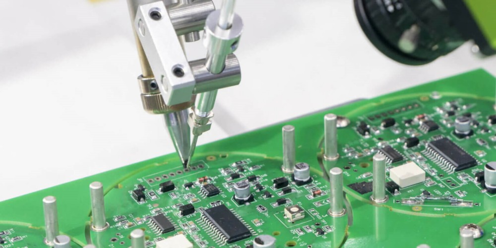
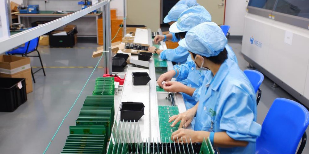
6. PCB Assembly
Components are soldered onto the fabricated PCB either manually or using automated assembly lines. This produces a functional electronic circuit.
7. Testing
The assembled PCBs undergo electrical and functional testing to ensure conformity to specifications. Debugging is done if issues are found.
Types of PCBs
There are several types of PCBs used in the electronics industry:
- Single-sided – Cu traces on one side of dielectric substrate
- Double-sided – Cu traces on both sides
- Multilayer – Multiple Cu/dielectric layers with plated through holes
- HDI – High Density Interconnect with microvias
- Rigid – Standard solid fiberglass based PCBs
- Flex – Flexible PCBs using polyimide substrates
- Rigid-Flex – Combination of rigid and flex sections
PCB Materials and Components
Some key materials and components used in PCB manufacturing are:
- Substrate – FR-4 (fiberglass + epoxy), Polyimide, PTFE, Alumina etc.
- Conductor – Copper, Silver, Gold etc.
- Solder Mask – LPI, Dry Film etc.
- Finish – HASL, Immersion Tin, ENIG, Silver etc.
- Via Construction – Plated Through Hole (PTH), Microvias, Buried vias etc.
- Components – Resistors, Capacitors, ICs, Transistors, Connectors etc.
The materials and construction methods used determine the performance and cost characteristics of the PCB.
Key Advantages of Using PCBs
Some benefits of using PCBs:
- Compact and reliable – PCBs allow dense component mounting and rugged mechanical assembly.
- Efficient power distribution – The planar construction ensures low impedance power distribution.
- Effective heat dissipation – PCBs can conduct heat efficiently from components.
- Design reusability – Modular PCB assemblies can be reused across products.
- Automated assembly – Components can be machine-placed and soldered efficiently.
- Reduced wiring errors – PCBs eliminate complex manual wiring between points.
- Miniaturization – Compact PCB constructions like HDI allow highly miniaturized circuits.
- Noise reduction – PCB ground planes help reduce electrical noise.
PCB Design Considerations
Some key factors to consider during PCB design:
- Electrical constraints – Track widths, clearances, impedances, losses, noise etc.
- Manufacturing capabilities – Minimum track/gap sizes, via types, layer count etc.
- Component placement – Optimize placement for routing, thermal and EMI considerations.
- Routing – Ensure shortest routes, matched lengths, avoid crosstalk etc.
- Thermal design – Heat dissipation, thermal vias, sinks etc.
- Mechanical constraints – Board shape, mounting holes, stiffness etc.
- Test points – Provide testpoints to validate circuits.
- Future modifications – Allow space for potential component changes.
- Cost – Simplify layouts, reduce layer count to optimize cost.
Careful consideration of these aspects ensures good performance, manufacturability and cost-effectiveness.
PCB Mass Production
For commercial electronic products, PCBs need to be mass produced. Some key aspects of PCB mass production:
- Volume pricing – Unit pricing reduces significantly with volume due to economies of scale.
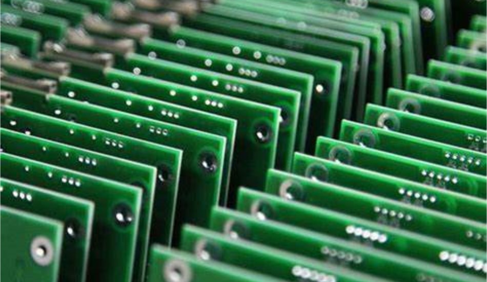
- Panelization – PCBs are grouped in large panels for fabrication.
- Automated assembly – SMT lines are used for automated component placement and soldering.
- Testing and QA – Automated Optical and Electrical Testing is conducted.
- Certifications – Manufacturers may have ISO certifications indicating process quality.
- DFM practices – Design for Manufacturing guidelines are followed to optimize manufacturability.
- Supply chain – Good inventory management ensures timely material supply.
- Lean manufacturing – Production processes are optimized by eliminating waste.
Choosing manufacturers with capabilities tailored for volume production is key for cost-effective PCB mass production.
Applications of PCBs
Some major applications of PCBs:
- Computers – Motherboards, expansion cards, power circuitry etc.
- Consumer Electronics – Smartphones, TVs, home appliances, gaming consoles etc.
- Automotive – Engine control units, infotainment systems etc.
- Industrial – PLCs, process control systems, robotics.
- Medical – Diagnostic systems, imaging equipment, heart monitors etc.
- Aerospace and Defense – Avionics systems, weapon systems etc.
- Communications – Networking hardware, telecom infrastructure.
- IoT Devices – Smart home products, wearables, sensors etc.
Advancements in PCBs have enabled the miniaturization and performance improvements across virtually all electronics over the past decades.
Latest Trends in PCB Technology
Some latest trends shaping PCB technology are:
- HDI PCBs – Higher routing density with microvias and thinner traces.
- Any-layer HDI – Complex routing with microvias between any layers.
- Embedded passives – Passive components like resistors and capacitors integrated into the PCB.
- Flex and rigid-flex PCBs – PCBs integrating flexible and rigid sections.
- Advanced PCB Materials – Improved thermal and electrical performance.
- Additive processing – Additive fabrication of traces instead of etching to save material.
- 5G communication – PCBs for mmWave and high-frequency applications.
- PCB Embedded Electronics – Components embedded into the PCB for space savings.
- Automated assembly – Continuous improvements in automated SMT assembly.
- Green manufacturing – Processes that minimize wastage of materials and chemicals.
These innovations enable PCBs with higher performance, greater reliability and capabilities.
Conclusion
In summary, PCBs are indispensable structures that enable assembly and interconnection of electronic components. They provide the vital electrical and mechanical foundation for all electronic products. PCB manufacturing involves design, prototyping, fabrication and assembly processes to transform circuit requirements into functional boards. Careful consideration of electrical, thermal, mechanical and manufacturability constraints during design is key. With mass production, PCBs can be manufactured cost-effectively. Continued developments in PCB technology and assembly will enable faster, denser and higher performance electronic products.
Frequently Asked Questions
Q1. What are the different types of PCBs?
The main types of PCBs based on construction are:
- Single-sided – Conductors only on one side
- Double-sided – Conductors on both sides
- Multilayer – Multiple conductive layers stacked using dielectric
- HDI – High Density Interconnect with microvias
- Rigid – Standard solid PCBs
- Flexible – Flex PCBs using polyimide
- Rigid-flex – Combining rigid and flexible sections
Q2. What is the difference between PTH and microvias in PCBs?
PTH (Plated Through Holes) are standard plated holes that electrically connect different layers in multilayer PCBs. Microvias are smaller plated laser drilled holes with diameters typically less than 150 microns used to provide interlayer connections in HDI boards. Microvias enable thinner dielectric layers and higher component densities.
Q3. What are some advanced PCB substrate materials?
Some advanced substrate materials used in high performance PCBs are:
- PTFE (Teflon) – High frequency applications
- Ceramics like Alumina and Aluminum Nitride – High thermal conductivity
- FR-5 and FR-6 – High glass transition temperature
- Polyimide – Flexible PCBs
- LCP (Liquid Crystal Polymer) – Low loss, stable electrical performance
Q4. What are embedded passives in PCBs?
Embedded passives are passive components like resistors and capacitors that are integrated directly into the inner layers of PCB substrate itself instead of being mounted separately. This saves significant space compared to surface-mount passives.
Q5. How are PCBs typically tested?
Some common testing methods for PCBs are:
- Visual inspection – Verify PCB quality as per IPC standards
- In-circuit testing – Check for opens, shorts, faulty components
- Functional testing – Validate complete circuit/system operation
- Burn-in testing – Running boards at high temperature over time to check robustness
- E-test – Apply voltage spikes to verify insulation resistance
- X-ray imaging – Detect buried flaws and defects in inner layers


Leave a Reply