Introduction
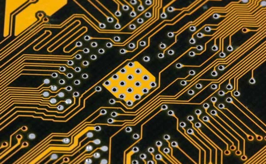
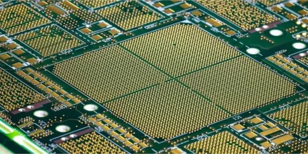
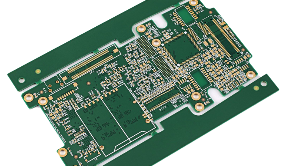
HDI (High Density Interconnect) is a printed circuit board (PCB) manufacturing technology that enables higher interconnect density and finer traces and spaces than conventional PCBs. HDI allows for more compact PCB designs by reducing the distance and pitch between traces and pads.
In a traditional PCB, there is only one interconnect layer between the top and bottom outer layers. HDI boards have two or more internal circuitry layers between these outer layers. The additional layers allow HDI PCBs to accommodate more tightly spaced traces and smaller vias.
Benefits of HDI Technology
Here are some of the key benefits of HDI PCBs:
- Higher interconnect density – More traces can be routed in the same area compared to conventional PCBs. This enables miniaturization and more compact designs.
- Finer lines and spaces – HDI processes allow for finer trace widths and spaces down to 2 mils. Standard PCB trace widths are 8 mils or more.
- Higher I/O density – The finer features allow for dense pin grids and high I/O components to be used.
- Better high speed performance – The tightly spaced traces, thinner dielectric layers, and buried vias in HDI boards provide better impedance control for high speed signals.
- Reduced layer count – HDI technology allows complex designs to be implemented with fewer layers due to the higher routing density.
- Lower costs – HDI provides cost savings for high volume production. Fewer layers lower costs.
- Miniaturization – HDI enables smaller and thinner end products due to increased PCB density.
HDI Buildup Layers
HDI PCBs achieve the high density and fine features through the use of additional buildup dielectric and trace layers. Here are some key terms related to HDI buildup:
- Core – The core is typically a standard FR4 dielectric layer that forms the main structure of the PCB. It is like the core of a conventional PCB.
- Buildup dielectric – Additional thin dielectric layers added on top of the core through a lamination process. These are typically 25-50 μm thick.
- Buildup traces – Fine linewidth copper traces patterned on top of the buildup dielectric layers. Multiple trace layers are separated by dielectric.
- Laser vias – Small diameter vias formed by laser drilling through the buildup layers to interconnect traces. These are 25-60 μm in diameter.
- Capture pads – Pads on the surface of the core dielectric layer to capture and interconnect with buildup vias.
This diagram shows a cross section of a simple 4 layer HDI board with 2 buildup layer pairs above and below the core:
| Layer | Description |
|---|---|
| Buildup Traces 2 | Outermost buildup trace layer |
| Buildup Dielectric 2 | Buildup dielectric layer |
| Buildup Traces 1 | Inner buildup trace layer |
| Buildup Dielectric 1 | Buildup dielectric layer |
| Core | Central FR4 core layer |
| Buildup Dielectric 1 | Buildup dielectric layer |
| Buildup Traces 1 | Inner buildup trace layer |
| Buildup Dielectric 2 | Buildup dielectric layer |
| Buildup Traces 2 | Outermost buildup trace layer |
The core forms the basic structure while the buildup layers on both sides provide the fine features and dense trace routing.
HDI Design Rules
To achieve the high density and electrical performance, HDI PCBs require adherence to tighter design rules compared to standard PCBs:
- Trace/Space – 4 mil line / 4 mil space is common on outer layers. 2 mil /2 mil trace/space on inner layers.
- Minimum annular ring – 4 mil diameter annular pad for laser vias
- Laser via size – Typically 25-60 μm diameter (1-2 mils)
- Laser via spacing – 150 μm minimum between laser via centers
- Capture pads – Capture pads are typically 4-8 mil diameter to intercept buildup laser vias
- Dielectric thickness – Thinner dielectrics of 25-50 μm used in buildup vs 100 μm for core
- Finished via – Laser via + capture pad = finished via. Must meet minimum annular ring design rules.
Adhering to these tighter design guidelines is critical to achieving a manufacturable HDI board.
HDI Materials
HDI PCBs require specialized materials engineered to enable the laser drilling, thinner dielectrics, and fine features.
- Core dielectric – FR4, high Tg FR4, polyimide, or thermoset laminates. Thickness typically 100 μm.
- Buildup dielectric – Thin film dielectrics like Ajinomoto Buildup Film (ABF), epoxy acyclic resin, polyimide. 25-50 μm thick.
- Copper – Rolled-annealed or electro-deposited copper foils. Very low profile and smooth foils used.
- Laser via drilling – CO2 or UV lasers used for drilling vias in buildup layers.
- Semi-Additive Process (SAP) – SAP method used to pattern dense fine line buildup traces.
HDI Substrate Types
There are two main substrate types used in HDI designs:
1. Sequential Lamination HDI
In sequential lamination HDI, the core and buildup dielectric layers are laminated one at a time in a sequential process. Advantages include:
- Simpler process with standard materials
- Lower cost
- Only need to laser drill the outermost buildup layers
However, there are some disadvantages:
- More susceptible to thickness variations
- Requires plated through holes (PTHs) for interconnections
- Not optimized for high density
2. Any-Layer HDI
Any-layer HDI can laser drill vias on any layer by using laminated one-piece dielectric cores. The main benefits include:
- Optimized for maximum density
- Buried vias improve routability and high speed performance
- Thinner and more stable dielectric thicknesses
The any-layer process is more complex but enables the highest density HDI designs with the best performance.
HDI Via Structures
There are several types of via structures used in HDI boards to interconnect layers:
- Microvias – Small laser drilled vias in buildup layers, typically 25-60μm diameter. Sometimes called as blind or buried vias.
- Through vias – Drilled through entire PCB thickness to interconnect outer layers. Typical for sequential lamination.
- Buried vias – Blind vias that do not extend to an outer surface. Used heavily in any-layer HDI.
- Stack vias – Used to connect multiple layers by stacking laser drilled microvias.
This diagram illustrates the various HDI via structures:
| Via Type | Description | Cross Section |
|---|---|---|
| Microvia | Small diameter laser drilled via in buildup layer | <img src=”https://files.mtstatic.com/site_4334/17966/0/Laser-Microvia.gif” width=”200″> |
| Through Via | Mechanically drilled through entire board | <img src=”https://files.mtstatic.com/site_4334/18028/0/ht18_xfaqs2_image3.gif” width=”200″> |
| Buried Via | Blind laser via connecting inner layers | <img src=”https://files.mtstatic.com/site_4334/18028/0/ht18_xfaqs5_image2.gif” width=”200″> |
| Stack Via | Stacked microvias connecting many layers | <img src=”https://files.mtstatic.com/site_4334/17966/0/stackvia.gif” width=”200″> |
HDI Design and Fabrication
Designing and manufacturing HDI PCBs requires special processes and considerations:
- Board layout – Must follow HDI design rules for lines/spaces, via sizes, capture pads, etc.
- Stackup planning – Determine the number of buildup layers needed to route design. Plan entire layer stackup.
- Laser via drilling – CO2 or UV lasers used to ablate microvias in buildup layers.
- Semi-Additive Process – SAP method used to pattern fine line traces in buildup layers.
- Sequential lamination – Core and buildup layers laminated one at a time. Or use pre-pressed 1-piece cores.
- Copper plating – SAP, panel plating, pattern plating used to plate vias and traces.
- Solder mask – LPI or dry film solder mask processes able to meet tight Tolerances.
- Final finishes – OSP, ENIG, immersion silver or gold used. Tests for porosity and black pad.
HDI fabs require specialized equipment, processes, and expertise to reliably manufacture these boards cost effectively.
Applications of HDI Technology
Some of the key application areas of HDI PCB technology include:
- Smartphones – Miniaturization and high I/O density needed. HDI provides compact interconnect.
- Wearables – Small, lightweight PCBs with high density interconnects.
- Medical – Implantables and compact instruments benefit from HDI density.
- Automotive – Advanced driver assistance systems and infotainment applications.
- Aerospace – Avionics systems with size and weight constraints.
- Computing – Tablets, notebooks, and computing require small and dense PCBs.
Any product that needs to be compact, lightweight, or high performance can benefit from utilizing HDI PCB technology. The high density routing and smaller vias provide advantages over conventional PCBs.
HDI PCB Challenges
While HDI offers many benefits, there are some challenges and considerations when working with HDI boards:
- Tighter design rules – Requires adjustments to layout practices to accommodate finer features.
- Need for high precision – Tighter tolerances across PCB fabrication processes.
- Potential for reduced yields – Dense boards more prone to defects. Need for thorough testing.
- Special materials – More exotic materials needed to achieve laser drilling and thinner dielectrics.
- Higher fabrication costs – More complex processing increases tooling and production costs.
- Limited supplier base – Only high-end PCB shops able to manufacture advanced HDI.
- Thermal management – Dense boards need careful thermal design due to higher heat densities.
Working closely with an experienced HDI PCB supplier is key to overcoming these challenges and ensuring a robust, high yielding board design and fabrication process.
HDI PCB Cost Considerations
Due to the higher fabrication complexity, HDI PCBs generally have a cost premium over conventional PCBs. Here are some of the key cost drivers:
- Number of HDI layers – More complex layer stacks increase costs.
- Board thickness – Thicker boards cost more due to longer drilling, plating, etc.
- Board size – Larger boards have higher material costs.
- Feature size – Finer lines & spaces and higher densities add cost.
- Special materials – Advanced materials like laser drillable films cost more.
- Lower yields – Dense designs may have lower yields, increasing cost.
- Tooling and setup – New designs require more engineering time.
- Small volume – Low volume HDI orders carry higher cost per board.
- Testing – Need for intensive inspection and electrical test adds cost.
HDI enables much smaller and higher performance PCBs, but designers should weigh the benefits vs. the increased fabrication costs depending on volumes and budget.
Summary
- HDI provides interconnect density improvements over conventional PCBs through finer traces, spaces, and multiple buildup layers.
- Key benefits include higher I/O density, smaller vias, improved performance, and miniaturization.
- HDI requires tighter design rules, advanced materials and processes, and additional cost considerations.
- Leading applications include consumer electronics, wearables, medical, automotive, and aerospace designs.
Frequently Asked Questions
Here are some common questions about HDI PCB technology:
What are the key advantages of HDI PCBs?
The main benefits of HDI technology are higher routing density, smaller vias, thinner dielectrics, and the ability to incorporate buried and blind vias. This enables improved electrical performance, higher component densities, miniaturization, and lower layer counts.
What are the minimum trace/space values achievable with HDI?
On outer layers, 4 mil lines and 4 mil spaces are readily achievable with HDI. On internal layers, 2 mil line/space is common. This depends on board fab process capabilities.
Are there any special DFM guidelines for HDI PCBs?
Yes, HDI designs require tighter design rules and considerations regarding line widths, spacing, minimum annular rings, capture pads, and via spans. Close collaboration with your PCB manufacturer is recommended.
Can microvias reliably interconnect 16+ layers in an HDI stackup?
Yes, with a well designed HDI layer stack and high precision PCB fab processes, interconnects with 20+ layers can be reliably achieved using stacked microvias.
What are the key reliability risks to watch out for with HDI?
Some of the key concerns are reduced solder joint reliability due to thinner dielectrics, potential for plating voids in microvias, thermomechanical fatigue, and coefficient of expansion mismatch issues.


Leave a Reply