
Introduction
Printed circuit boards (PCBs) are the backbone of modern electronics. They provide the electrical connections and pathways between components mounted on the board. To connect components and routing signals between layers of the PCB, plated through holes called vias are used.
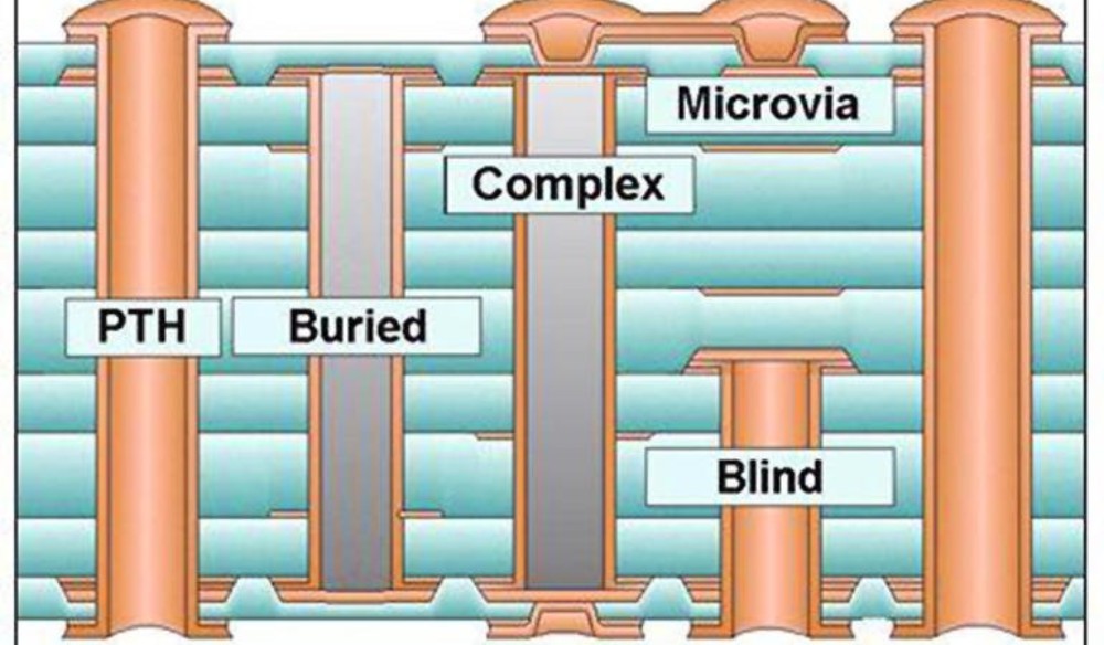
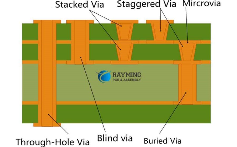
Vias can be through-hole vias that span the entire thickness of the PCB or blind/buried vias that connect only some of the layers. Buried vias are a type of blind via constructed internally between the layers of the PCB without reaching the outer surfaces. They provide interlayer connections without using up valuable surface real estate.
What are Buried Vias?
Buried vias are plated through holes that connect two or more internal layers of a multilayer PCB without connecting to the outer layers. They are fabricated by drilling holes on the inner layers that need to be connected, metallizing the hole walls, and then laminating outer layers over them.
Some key properties of buried vias:
- They provide connections between internal layers only, without using up surface area like through-hole vias.
- High density routing capabilities by reducing surface clutter.
- Improved signal integrity at high frequencies compared to through-hole vias.
- Require more complex PCB fabrication process.
- More expensive than standard vias due to complex lamination process.
- Size range from 0.1mm to 0.25mm diameter generally.
Applications of Buried Vias
Buried vias have some unique advantages that make them suitable for certain PCB applications:
High Density Interconnects
In complex multi-layer boards with high routing density, buried vias can relieve congestion on the outer layers. They provide short and efficient interconnects between inner layers without using valuable surface real estate.
RF Circuits
In radio frequency (RF) circuits, buried vias can provide better performance compared to plated through-hole vias. Their shorter length gives lower inductance, while being buried inside the board shields them from interfering with sensitive RF signals.
Mixed Signal PCBs
For mixed signal designs with both analog and digital circuits, buried vias allow segregating analog and digital routes internally. This improves signal integrity by avoiding noise coupling between analog and digital signals.
LED PCBs
In LED PCBs, buried vias can connect the inner layer ground planes to the LED pads. This provides a thermal path for conducting heat away from the LEDs, improving their performance and lifespan.
High Speed Designs
In high speed designs, buried vias can minimize unwanted impedance mismatches and discontinuities as signals propagate between layers. Their shorter length gives lower inductance for cleaner high speed signals.
How are Buried Vias Constructed?
The fabrication process of a PCB with buried vias involves several steps:
- Drilling holes on the required inner layer pads where interlayer connections are needed.
- Metallizing the drilled holes through electroless copper plating to form a conductive coating on the hole walls.
- Aligning outer layer laminates over the plated holes and bonding them using high temperature and pressure. This encapsulates the plated holes inside the board.
- Drilling holes for through vias as needed to connect outer layers.
- Plating the board edge walls and all holes to form a conductive connection between layers.
- Machining the board outline and finished thickness.
- Solder mask, silkscreen, finish plating steps.
This multi-step lamination process requires precise alignment between layers and advanced PCB fabrication capabilities.
Pros and Cons of Using Buried Vias
Here are some key advantages and disadvantages of using buried vias:
Advantages
- Frees up space on outer layers by moving interlayer connections inside.
- Allows higher routing density and component placement flexibility.
- Shorter interconnect length gives better high frequency response.
- Shielding from outer layers reduces EMI/RFI effects.
- Allows segregating analog and digital routes on inner layers.
Disadvantages
- More complex fabrication process increases cost.
- Require advanced PCB manufacturing capabilities.
- Difficult to visually inspect or probe if defects occur.
- Repair and rework is challenging.
- Adds constraints on layer stackup and layout arrangement.
Design Guidelines for Buried Vias
Here are some key guidelines to follow when designing with buried vias:
- Minimize use of buried vias as they impact manufacturability and cost. Use only when necessary.
- Maintain adequate annular ring width around buried via barrels. This ensures reliable plating thickness.
- Avoid placing buried vias under high density BGA packages as rework is difficult.
- Plan layer stackup so critical signals have shortest buried via length.
- Use larger capture pads when routing high speed signals through buried vias.
- Verify buried via placement with manufacturer’s capabilities before finalizing layout.
- Plan cutouts in ground planes under buried vias carrying sensitive analog or RF signals.
Comparison between Buried Vias, Blind Vias and Through Vias
| Parameter | Buried Vias | Blind Vias | Through Vias |
|---|---|---|---|
| Definition | Connect internal layers only | Connect outer layer(s) to internal layer(s) | Connect all layers from top to bottom |
| PCB Real Estate | Saves space on outer layers | Saves some space on outer layers | Uses maximum space on outer layers |
| Manufacturing | Very complex process | Moderate complexity | Simple basic process |
| Cost | Very High | Moderate | Low |
| Signal Performance | Best due to minimum length | Better than through vias | Worst due to maximum length |
| EMI/RFI Shielding | Fully shielded inside PCB | Partial shielding | No internal shielding |
| Thermal Conduction | Poor | Moderate | Best |
| Inspection | Not possible | Partial inspection | Full inspection possible |
| Repair/Rework | Extremely difficult | Possible with some effort | Simplest process |
Frequently Asked Questions (FAQs)
Here are some common FAQs about buried vias:
Q: What is the typical size range of buried vias?
A: Buried vias typically range from 0.1 mm to 0.25 mm in diameter. High density designs may use vias down to 0.05 mm. The size depends on PCB fabrication capabilities.
Q: Can buried vias be stacked (vias within vias)?
A: Yes, stacked or staggered buried vias are possible, but require very advanced manufacturing processes and increase cost significantly.
Q: Are buried vias only used on high density PCBs?
A: Not necessarily, they can be useful in many designs from 4-6 layers upwards to provide interlayer connections without consuming surface space.
Q: Do buried vias affect the reliability or longevity of a PCB?
A: If designed properly with good fabrication quality, buried vias are very reliable interconnects. Their internal structure is well protected from environmental stresses.
Q: How are buried vias tested for manufacturing defects?
A: Electrical testing using flying probe or bed-of-nails test fixtures is commonly used. X-ray imaging can also reveal potential voids or flaws in buried plating.


Leave a Reply