Introduction
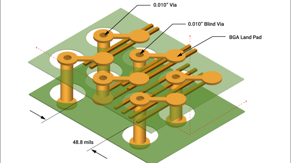
In printed circuit boards (PCBs), a blind via is a hole that connects different layers of a multi-layer PCB without going through the entire board. Blind vias are used to route connections between internal layers of a PCB without using up space on the outer layers. They allow designers to route traces more efficiently and optimize board space on high density PCBs.
Blind vias are an important tool for designing complex, compact PCBs. In this article, we will cover what blind vias are, how they differ from other via types, their key benefits, design considerations, and some examples of how they are used in PCBs.
What is a Blind Via?
A via is a plated hole in a PCB that provides an electrical connection between different layers. Vias can pass all the way through from the top to the bottom layer (through-hole via), or they can connect only between some internal layers (blind/buried vias).
A blind via connects one or more internal copper layers of a PCB without connecting to the outer layers on the top or bottom of the board. It is blind from the outer surfaces – it cannot be seen looking down vertically from the top or bottom layer.
Some key characteristics of blind vias:
- Connects two or more internal copper layers.
- Does not connect to the outer copper layers.
- Not visible looking vertically from the surface of the PCB.
- Often requires careful alignment between layers.
- Allows routing signals between internal layers only.
- Requires high accuracy drilling and plating.
Blind vias are often used in dense, multilayer boards to optimize routing and layer usage. The name comes from being ‘blind’ to the surface layers.
Difference Between Blind, Buried, and Through-Hole Vias
There are three main types of vias in PCBs:
- Through-hole via: Goes all the way through from the top to bottom layer.
- Blind via: Connects internal layers only, without reaching the top or bottom surface.
- Buried via: Starts and ends on internal layers without connecting to the outer surfaces.
The key differences are:
| Via Type | Connects Outer Layers | Connects Inner Layers | Visible from Surface |
|---|---|---|---|
| Through-hole | Yes | Yes | Yes |
| Blind | No | Yes | No |
| Buried | No | Yes | No |
Through-hole vias are the most common type – they go through the entire PCB from top to bottom. This allows them to connect traces on the outer layers and provides continuity through the whole board.
Blind vias only connect internal layers. They allow traces to transition between internal layers without using up space on the crowded outer layers. Blind vias are invisible from the top or bottom of the board.
Buried vias are similar to blind vias but do not connect to either of the outer surfaces. They are ‘buried’ entirely within internal layers. These are only used on boards with four or more layers.
Benefits and Uses of Blind Vias
Using blind and buried vias provides several key benefits for PCB design:
1. Frees up space on outer layers: By routing connections internally, blind vias reduce congestion on the top and bottom layers. This is especially useful in dense, multilayer boards.
2. Allows more routing channels: With access to internal layers, traces can be routed between components more efficiently. This facilitates routing for complex designs.
3. Optimizes layer usage: Different layers can be dedicated to specific signals types, such as power or ground planes. Blind vias allow judiciously transitioning between layers.
4. Reduces via stub effects: Stub effects from through-hole vias are avoided, improving signal performance at high frequencies.
5. Improves manufacturability: Smaller blind vias take up less space and are easier to produce than large through-hole vias.
Here are some examples of using blind and buried vias in PCBs:
- High speed design: Blind vias allow high-speed signals to stay on internal layers, avoiding discontinuities and maintaining trace impedance.
- RF PCBs: Blind and buried vias are used to route signals within stripline RF transmission lines. This avoids radiation and signal loss.
- Multi-layer boards: They help optimize trace routing between many layers of dense, complex boards.
- HDI PCBs: High density interconnect (HDI) boards with microvias rely heavily on blind and buried vias for layer transitions.
- IC connections: Blind and buried vias are ideal for connecting BGA packages or dies directly to internal routing layers.
Overall, using blind and buried vias allows for more efficient use of layers, enabling complex and compact multi-layer PCB designs. The high density and small sizes make them ideal for advanced PCB technologies.
Design Considerations for Blind Vias
While blind vias provide many benefits, the design must accommodate their unique requirements:
1. Alignment between layers: The layers connected by a blind via must be carefully aligned to ensure the via connects the proper pads on each layer.
2. High aspect ratio: Blind vias often have a higher aspect ratio than through-hole vias. This makes plating the blind via barrel more difficult.
3. Limited redundancy: A blind via provides only one connection path between layers. If it fails, there is no backup through other layers.
4. Testing challenges: Since they are not accessible from the outer surface, blind vias cannot be directly probed for testing.
5. Via stub effects: Stubs from blind vias can still impact high-speed signals so length should be minimized.
6. Fabrication constraints: Blind vias require advanced drilling and plating capabilities, along with tight process controls. Not all fabricators can produce them.
With careful design techniques like using fat pads around blind vias, adding redundancy, simulating performance, and working closely with your fabricator, the risks of using blind vias can be minimized.
PCB Layer Stackup Options with Blind Vias
Blind vias are commonly used in advanced multilayer boards. Here are some typical layer stackup configurations that employ blind and buried vias:
4-layer board with blind vias:
- Blind vias connect Layer 1 and Layer 2 routed signals.
- Through-hole vias connect all layers.
6-layer board with blind and buried vias:
- Blind vias connect Layers 1-2, 2-3, 4-5, and 5-6.
- Buried vias connect Layers 2-4 and 3-5.
8-layer HDI board:
- Uses microvias to connect high density build-up layers.
- Buried vias route signals between internal high speed layers.
- Blind vias connect build-up layers to inner layers.
Using a combination of blind, buried, and through-hole vias provides maximum flexibility in complex PCB stackups.
Example Applications of Blind Vias
Here are some examples of blind vias used in real-world PCBs:
1. High speed DDR memory routing
Blind vias allow precise routing of DDR memory buses to inner layers, separating them from other signals. Stub lengths are minimized and impedance is tightly controlled.
2. BGA fanout
Dense signal fanout from a BGA can be routed internally using blind and buried vias. This avoids congestion on outer layers under the package.
3. RF stripline transmission lines
Blind vias allow RF traces to transition between reference ground layers, creating shielded stripline transmission lines.
4. LED display panels
LED mounting holes are connected to inner layers using blind vias. This keeps the top and bottom clear of vias and components.
5. IC and package transitions
Using blind/buried vias provides a direct interface from ICs and packages to internal routing layers. This optimizes layer usage.
Blind Via PCB Fabrication Process
Fabricating PCBs with blind vias requires specialized manufacturing capabilities:
Drilling: Laser drilling can create small blind vias with high accuracy. Mechanical drilling may be used for larger blind vias. Depth control is critical.
Metallization: Blind vias are plated to metallize the barrel using electroless copper and then electroplated copper. Specialized plating processes ensure uniform plating.
Lamination: Careful layup and lamination alignment is needed so blind via locations match between layers. Step-laminate processes build up sub-sections.
Testing: Electrical testing uses flying probe testers or x-ray inspection. Since blind vias are not accessible, testing requires specialized techniques.
Quality Control: Regular optical and x-ray inspection confirms blind via structure. Automated optical inspection looks for defects or misalignments.
Fabricators invest in advanced equipment and processes like laser direct imaging (LDI), plasma etch, and x-ray laminate drilling to produce boards with blind and buried vias. Close partnerships with designers is key for manufacturability.
Frequently Asked Questions
Here are some common questions about blind vias in PCBs:
Q: Can blind vias be repaired if defective?
A: It is very difficult if not impossible to repair a defective blind via. If issues are detected during fabrication, the entire PCB build may have to be scrapped. Redundant vias can help mitigate this risk.
Q: What is the typical size range of blind vias?
A: Blind vias can range from small microvias around 0.15mm up to around 0.4mm for high density interconnects. Large mechanical blind vias above 0.6mm are also possible.
Q: How are blind vias tested if they are not visible?
A: Electrical testing can detect connectivity faults. X-ray imaging is used to inspect internal blind via structure and alignments during fabrication.
Q: Can blind vias be filled?
A: Yes, blind vias will typically get filled with epoxy or other materials to provide mechanical stability, though some high frequency designs may leave them unfilled.
Q: What fabrication technologies are best suited for blind vias?
A: Laser based processes such as laser drilling and LDI offer the precision required for blind vias. Advanced x-ray based inspection is also critical.
Conclusion
Blind vias are a key enabling technology for advanced, multi-layer PCB designs. By providing direct connections between internal layers, they optimize routing capabilities and layer usage in complex boards. While requiring careful design considerations, blind vias allow engineers to produce highly integrated PCBs for cutting-edge applications. As PCB technology continues advancing into HDI and beyond, the use of blind and buried vias will become even more widespread.


Leave a Reply