Introduction
HDI (High Density Interconnect) is a term used to describe printed circuit boards (PCBs) with a higher wiring density than traditional boards. HDI allows for tighter spacing and smaller traces and vias, enabling more interconnects in a given area. This allows HDI PCBs to accommodate more complex circuitry in a smaller footprint, which is especially important for compact, high-performance electronic devices.
In this article, we will explore what HDI means, its key characteristics, fabrication methods, and applications. Understanding HDI technology is important for electrical engineers and PCB designers working on miniaturized, cutting-edge products.
What Does HDI Stand For?
HDI stands for High Density Interconnect. It refers to a style of multilayer PCB with fine features and high component density.
Specifically, HDI has:
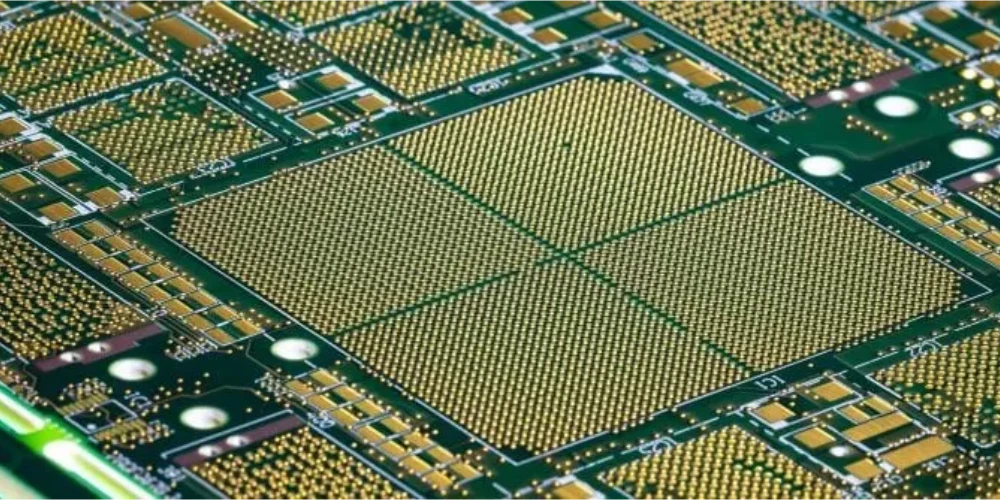
- Smaller trace widths and spacing (5 mils or less)
- Microvias with smaller diameters (6 mils or less)
- Thinner dielectric layers (3 mils or less)
This allows routing of more signals in less space compared to standard PCB technologies. HDI stacks multiple thin dielectric layers rather than one thick core, facilitating high interconnect density.
The term HDI was coined by the IPC (Association Connecting Electronics Industries) to denote PCBs meeting certain density requirements. IPC-2226A specifies the design guidelines for HDI boards.
Key Characteristics of HDI PCBs

Here are some of the typical characteristics of HDI boards:
- Trace Width/Spacing: 4 mils or smaller
- Microvia Diameter: 6 mils or smaller
- Dielectric Layer Thickness: 2-3 mils
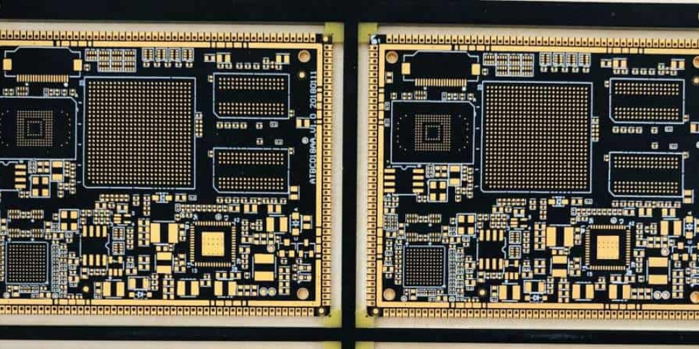
- Number of Routing Layers: 6+ layers
- Line/Space Ratio: Up to 20:1
- Via Pad Size: 8-12 mils with 6-8 mil microvias
- Finished Copper Thickness: 0.7-1.4 mils
This combination of fine features enables routing tracks with 4 mil width and spacing in 6-8 conductive layers. A board with 8 mil line and space would have 10-12 routing layers.
HDI architecture allows at least 20% more routing channels compared to conventional PCBs. This boosts interconnect density and component packaging.
Key Advantages of HDI
The miniaturized dimensions achieve the following benefits:
- Higher interconnect density – More routing channels and vias per unit area
- Thinner profile – Overall board thickness under 100 mils
- Fine lines and spaces – Accommodates lead pitches under 8 mils
- High-speed performance – Tight signal control and impedance matching
- Efficient power distribution – Multiple power plane layers
- More passives – Allows embedding 0201 and 01005 passives
- Layer stackup flexibility – Optimize for SI, PI, or mixed designs
HDI Fabrication Process
Fabricating HDI boards requires specialized PCB processes to handle the nanoscale features involved. Here is an overview of how HDI boards are manufactured:
Tight Tolerance Layers
The buildup dielectric layers must be extremely uniform and consistently thin across each panel. Tight thickness tolerances (±10%) are necessary to control trace impedance and minimize crosstalk.
Advanced materials like thermoset polymers, polyimides, and liquid photo resins are used. Dielectrics are coated on copper foils using lamination or spin coating.
Fine Line Routing
To reliably produce 4-5 mil traces and spaces, photolithographic methods with tighter process controls are needed. Laser direct imaging (LDI) offers precise exposures for small features.
Solder masks and legend inks require similarly tight tolerances and registration accuracy. Thinner copper layers help enable fine features.
Laser Microvias
Blind and buried microvias with 6 mil diameters or less are essential in HDI. The vias are laser-drilled through tape layers before lamination. CO2 and UV lasers allow drilling microvias with 2-3 mil diameters.
Thin Core or Coreless Construction
Instead of a thick core layer, HDI boards use several paired thin dielectric films around 12-25 μm thick. This enables thinner overall board stacking. Coreless constructions with only buildup films are also possible.
Stackup Optimization
With multiple thin dielectric layers, HDI stackups can be optimized for high-speed, high-frequency, RF, or mixed signal requirements. Signal layers, power planes, and plane pairings are configured for electrical performance.
Sequential Lamination
Dielectric films and copper foils are laminated in pairs to build up the multilayer HDI board. Laser microvias are formed between each sequential lamination step. This allows great flexibility in trace routing and via connections.
Advanced Plating
To reliably plate ultra-thin walls of microvias, conformal copper plating processes like pulse plating are used. Copper is also plated to fill blind vias. This creates a continuous connection between layers.
Tight Process Controls
Manufacturing HDI PCBs requires stringent process controls to hold tight tolerances across panel sizes up to 18”x24”. Automated optical inspection (AOI) and testing ensures reliability.
HDI Board Applications
The specialty capabilities of HDI make it suitable for advanced electronics designs such as:
Consumer Mobile Devices
Smartphones, tablets, and wearables with constrained footprints widely use HDI boards. The high density accommodates components and interconnects within thin, compact platforms.
Internet of Things (IoT)
Connecting everyday objects requires packing communication modules and sensors into very small electronics. HDI allows routing complex IoT circuitry in a miniaturized PCB.
Automotive Electronics
Driver assistance systems, infotainment, and controls require dense, high-speed PCBs. HDI meets automotive reliability requirements while providing thin, flexible form factors.
Medical Devices
Implantable and wearable medical devices demand maximum functionality in a tiny package. HDI provides the interconnect density for complex microelectronics and sensors.
Aerospace and Defense
Mission-critical guidance systems, communications, and avionics for spacecraft and aircraft rely on HDI circuit integration. The boards provide fail-safe performance in harsh environments.
High-Speed Digital Designs
Servers, telecom/datacom, and test & measurement systems need advanced PCBs to handle multi-GHz signals. HDI facilitates dense routing and ultra-thin dielectrics for impedance control.
As electronic devices continue getting more complex and compact, HDI will become increasing prevalent across industries and applications.
HDI PCB Design and Layout
To effectively implement an HDI printed circuit board design, engineers need to follow specialized design rules and layout techniques. Here are some key points for HDI PCB design:
Follow IPC-2226A Guidelines
This IPC spec gives detailed HDI design guidance on trace widths, spaces, microvias, lamination, and more based on fabrication capabilities. This ensures designs are manufacturable.
Use Constraints for Nets and Components
Board layout tools should define 4 mil or 5 mil routing grids for traces along with 6 mil microvia sizes. Components are constrained to their recommended layout pads and pin areas.
Optimize Stackup
Model layer thicknesses and dielectric properties to configure an HDI stackup that meets impedance, signal quality, power, and EMI requirements. This is done during pre-layout planning.
Plan Power Distribution
Allocate multiple thin power plane layers to provide clean, steady power delivery to ICs. Use several lower voltage planes vs. one thick higher voltage plane.
Include Ground Planes
At least one continuous ground plane next to each signal layer is necessary to provide a return path and shielding. Multiple ground planes improve impedance control.
Use Blind and Buried Vias
Route signals between layers using blind or buried microvias, avoiding stub connections. Laser-drilled microvias enable connections in the middle of a PCB stackup.
Watch Transmission Line Lengths
Match trace lengths through layer changes to control propagation delays, prevent stubs, and reduce reflections. This is essential for multi-Gbps signals.
Verify Impedances
Run post-layout simulations to verify routing meets impedance targets across various layer transitions. Tune the stackup if needed.
Proper HDI layout techniques result in a manufacturable, high-performance board that makes full use of HDI capabilities.
HDI PCB vs Standard PCB Comparison
HDI offers many advantages over standard PCB technologies. Here is a comparison:
| Parameter | Standard PCB | HDI PCB |
|---|---|---|
| Dielectric Thickness | ~30-100 mils | 2-3 mils per layer |
| Traces/Spaces | ≥ 8 mils | ≤ 5 mils |
| Microvias | ≥ 15 mils | ≤ 6 mils |
| Line/Space Ratio | Up to 10:1 | Up to 20:1 |
| Routing Layers | 4-8 layers | 6-16 layers |
| Passive Integration | 0402, 0201 | 0201, 01005 |
| Impedance Control | Fair | Very tight |
| High-Speed Support | Multi-GHz | 10+ Gbps |
| Stackup Flexibility | Limited | Very versatile |
| Thickness | ≥ 100 mils | < 100 mils |
| Design Complexity | Medium | Very complex |
The miniaturization and performance benefits of HDI come at the cost of more complex design and fabrication processes. But for advanced electronics, HDI is enabling.
The Future of HDI Technology
HDI PCB technology will continue evolving to meet the needs of next-generation electronic products:
- Even smaller trace/space dimensions – reaching 2 mils
- Microvias below 5 mils diameter
- Thinner dielectric films below 1 mil
- Higher interconnect densities > 1000 traces/inch
- Embedding bare die and passives
- Multi-chip packages with HDI integration
- High-volume manufacturing on panel sizes over 24” x 24”
- Flex-rigid HDI boards
- Optical and RF integration
HDI will be key to realizing new applications in 5G communications, autonomous vehicles, AI, and other emerging industries.
Conclusion
HDI PCB technology enables the high component density, small form factors, and signal integrity needed in cutting-edge electronics. As products continue getting smaller and more complex, HDI will become a necessity.
Understanding what defines HDI, its fabrication, design, applications, and evolution is important knowledge for electrical engineers, PCB designers, and technical product managers. HDI advancements will power innovation across consumer, industrial, and military product spheres.
Frequently Asked Questions
What is the key benefit of HDI PCBs?
The main benefit of HDI is enabling higher routing density and component packaging within a given area by using thinner dielectrics, fine lines/spaces, and microvias. This allows for more compact and complex circuitry.
What are typical HDI board thicknesses?
HDI boards usually range from 60-100 mils thickness. Individual dielectric layers are 2-3 mils thick, much thinner than the ~30 mil cores used in standard multilayer boards.
Can HDI boards incorporate controlled impedance?
Definitely, the thin dielectrics and very tight process controls of HDI allow engineers to design controlled impedance transmission lines meeting specific impedance targets. This is critical for high-speed signal integrity.
Are there limitations on HDI board size?
Historically HDI fabrication was limited to smaller sizes, but advances in processes and laminate materials now allow HDI layers to be reliably manufactured on panel sizes exceeding 18”x24”. Large HDI boards are becoming common.
Does HDI improve signal quality?
The combination of thinner dielectrics, impedance control, dense power distribution, and ultra-short routing with microvias gives HDI boards very high signal and power integrity. This maintains signal quality and timing across even multi-Gbps links.


Leave a Reply