What is Solder Mask?
Solder mask, also known as solder resist or solder stop, is a thin layer of polymer applied to the surface of a PCB. It is typically green in color but can also be found in other colors such as red, blue, or black. The primary purpose of solder mask is to protect the copper traces on the PCB from oxidation, shorts, and damage during the soldering process and throughout the life of the electronic device.
The solder mask is applied to the PCB using various methods, including screen printing, liquid photo imaging, or dry film photoresist. The choice of application method depends on factors such as the desired thickness, precision, and production volume.
Functions of Solder Mask in PCB
1. Insulation and Protection
One of the primary functions of solder mask is to provide insulation and protection to the copper traces on the PCB. The solder mask acts as a barrier between the copper and the environment, preventing oxidation and corrosion that can degrade the performance of the circuit over time. Additionally, the solder mask protects the copper traces from physical damage, such as scratches or impacts, which can cause shorts or open circuits.
2. Solder Dam
Another essential function of solder mask is to act as a solder dam during the soldering process. The solder mask is designed to repel molten solder, preventing it from flowing onto unwanted areas of the PCB. This is particularly important for surface mount components, where precise solder joint formation is critical for proper functioning and reliability.
The solder mask defines the exposed copper areas where solder is meant to adhere, known as solder pads. By selectively exposing these pads while covering the rest of the copper traces, the solder mask ensures that solder only flows onto the intended areas, reducing the risk of shorts and bridges between adjacent traces.
3. Improved Current Carrying Capacity
Solder mask also plays a role in improving the current carrying capacity of PCB traces. When a PCB is designed, the width of the copper traces is calculated based on the expected current flow and the desired temperature rise. However, the presence of solder mask on top of the copper traces can effectively increase the cross-sectional area of the trace, allowing it to carry more current without overheating.
This is because the solder mask acts as an additional layer of insulation, reducing the amount of heat dissipated from the copper trace to the surrounding environment. As a result, the trace can handle higher current densities without experiencing excessive temperature rise, which can lead to improved reliability and longevity of the electronic device.
4. Enhanced Aesthetics and Legibility
In addition to its technical functions, solder mask also serves an aesthetic purpose in PCB design. The green color of the solder mask provides a clean and professional appearance to the PCB, making it visually appealing and easier to inspect. Moreover, solder mask can be used to create contrasting colors for component markings, labels, and other visual indicators on the PCB.
This enhanced legibility is particularly important for assembly and troubleshooting purposes. Clear and easily readable component designators, polarity markers, and test points on the PCB can significantly reduce the time and effort required for assembling and debugging the electronic device. The solder mask color can be chosen to provide optimal contrast against the silkscreen markings, ensuring that the information remains legible even under low light conditions.
5. Conformal Coating and Environmental Protection
In some applications, solder mask can also serve as a conformal coating, providing additional environmental protection to the PCB. Conformal coatings are thin layers of insulating material that conform to the contours of the PCB, shielding it from moisture, dust, and other contaminants.
While solder mask itself is not a true conformal coating, it can offer some level of protection against mild environmental factors. For example, solder mask can help prevent the ingress of moisture and humidity, which can lead to corrosion and electrical leakage. Additionally, solder mask can provide a barrier against light chemical splashes and dust accumulation, which can degrade the performance of the PCB over time.
However, for applications that require more robust environmental protection, such as in harsh industrial environments or outdoor settings, additional conformal coatings may be applied on top of the solder mask. These coatings, such as acrylic, silicone, or urethane, offer superior resistance to moisture, chemicals, and extreme temperatures, ensuring the long-term reliability of the electronic device.

Solder Mask Application Process
The application of solder mask to a PCB involves several steps to ensure proper coverage, adhesion, and precision. The process begins with the design of the solder mask layer in the PCB layout software. The solder mask layer defines the areas where the mask will be applied and the areas that will remain exposed, such as solder pads and test points.
Once the solder mask design is finalized, the PCB manufacturer prepares the board for solder mask application. This typically involves cleaning the surface of the PCB to remove any contaminants or oxidation that may interfere with the adhesion of the solder mask. The cleaning process may include chemical cleaning, plasma cleaning, or mechanical abrasion, depending on the specific requirements of the PCB and the solder mask material.
After cleaning, the solder mask material is applied to the PCB using one of several methods:
-
Screen Printing: In this method, a fine mesh screen is used to transfer the solder mask material onto the PCB. The screen has a stencil of the solder mask pattern, and the material is forced through the openings in the screen onto the board. Screen printing is suitable for high-volume production and can achieve a relatively thick solder mask layer.
-
Liquid Photo Imaging (LPI): LPI is a photolithographic process that involves applying a liquid solder mask material to the PCB and then exposing it to UV light through a photomask. The UV light cures the exposed areas of the solder mask, while the unexposed areas remain liquid and can be washed away. LPI offers high precision and can achieve thinner solder mask layers compared to screen printing.
-
Dry Film Photoresist: This method uses a pre-made film of solder mask material that is laminated onto the PCB. The film is then exposed to UV light through a photomask, curing the exposed areas. The unexposed areas are then removed using a chemical developer. Dry film photoresist is suitable for high-volume production and can achieve consistent solder mask thickness.
After the solder mask material is applied and cured, the PCB undergoes a final curing process to fully harden the solder mask and improve its adhesion to the board. This typically involves exposing the PCB to high temperatures in an oven or infrared heater for a specific duration.
| Solder Mask Application Method | Advantages | Disadvantages |
|---|---|---|
| Screen Printing | – Suitable for high-volume production – Can achieve thicker solder mask layers |
– Lower precision compared to other methods – Requires frequent screen maintenance |
| Liquid Photo Imaging (LPI) | – High precision – Can achieve thinner solder mask layers |
– Slower process compared to screen printing – Requires precise control of liquid solder mask viscosity |
| Dry Film Photoresist | – Suitable for high-volume production – Consistent solder mask thickness |
– Limited flexibility in solder mask design – Requires careful handling of the dry film material |

Solder Mask Materials
Solder mask materials have evolved over the years to meet the demands of modern PCB manufacturing. The choice of solder mask material depends on various factors, such as the intended application, environmental requirements, and compatibility with the PCB substrate and components.
Some common solder mask materials include:
-
Liquid Photoimageable Solder Mask (LPSM): LPSM is a liquid solder mask material that is applied to the PCB and then exposed to UV light to cure. It offers excellent adhesion, high resolution, and good resistance to chemicals and high temperatures. LPSM is widely used in the electronics industry due to its versatility and reliability.
-
Dry Film Solder Mask (DFSM): DFSM is a solid film of solder mask material that is laminated onto the PCB and then exposed to UV light to cure. It provides consistent thickness and high resolution, making it suitable for fine-pitch components and high-density PCB designs. DFSM is also known for its excellent resistance to chemicals and high temperatures.
-
Epoxy Liquid Solder Mask: Epoxy liquid solder mask is a two-part material that consists of an epoxy resin and a hardener. When mixed, the material is applied to the PCB and cured using heat. Epoxy solder mask offers excellent adhesion, high resistance to chemicals and moisture, and good thermal stability. It is often used in applications that require high reliability and durability.
-
UV Curable Solder Mask: UV curable solder mask is a single-part material that cures when exposed to UV light. It offers fast curing times, high resolution, and good resistance to chemicals and abrasion. UV curable solder mask is often used in high-volume production and applications that require quick turnaround times.
Each solder mask material has its own advantages and disadvantages, and the choice ultimately depends on the specific requirements of the PCB and the intended application.

Solder Mask Color Options
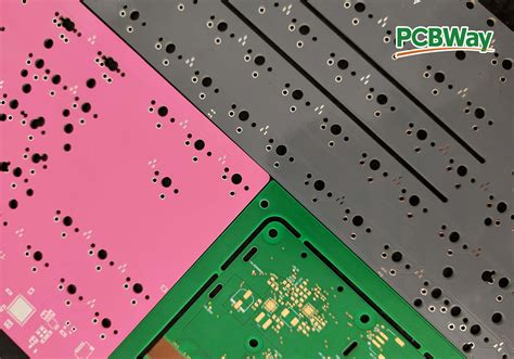
While green is the most common color for solder mask, PCB manufacturers offer a variety of color options to meet different aesthetic and functional requirements. Some popular solder mask color options include:
-
Green: Green is the default color for most solder masks and is widely used in the electronics industry. It provides good contrast against copper traces and is easily recognizable as a PCB.
-
Black: Black solder mask offers a sleek and professional appearance and is often used in high-end electronic devices. It provides excellent contrast against white silkscreen markings and can help hide any imperfections on the PCB surface.
-
Red: Red solder mask is often used in applications that require high visibility, such as emergency stop buttons or warning indicators. It can also be used for aesthetic purposes in consumer electronics.
-
Blue: Blue solder mask is becoming increasingly popular in the electronics industry due to its attractive appearance and good contrast against white silkscreen markings. It is often used in consumer electronics and IoT devices.
-
White: White solder mask is less common but can be used in applications that require a clean and minimalist appearance. It can also help reflect heat away from the PCB, making it suitable for high-temperature applications.
-
Yellow: Yellow solder mask is sometimes used in applications that require high visibility, such as in automotive electronics or industrial control panels.
In addition to solid colors, some PCB manufacturers offer custom solder mask colors and even patterns or images. These customization options can be used for branding purposes or to create unique visual effects on the PCB.
Frequently Asked Questions (FAQ)
-
What is the purpose of solder mask on a PCB?
Solder mask serves several purposes on a PCB, including providing insulation and protection to the copper traces, acting as a solder dam to prevent solder from flowing onto unwanted areas, improving current carrying capacity, enhancing aesthetics and legibility, and offering some level of environmental protection. -
Is solder mask necessary on all PCBs?
While solder mask is highly recommended for most PCBs, it may not be necessary for some simple or low-density designs. However, for the vast majority of modern electronic devices, solder mask is considered an essential component for ensuring reliability, performance, and longevity. -
What is the typical thickness of solder mask on a PCB?
The typical thickness of solder mask on a PCB ranges from 0.0005 to 0.002 inches (0.0127 to 0.0508 mm). The exact thickness depends on the specific solder mask material, application method, and PCB requirements. -
Can solder mask be removed from a PCB?
Yes, solder mask can be removed from a PCB using various methods, such as chemical etching, mechanical abrasion, or laser ablation. However, removing solder mask should only be done when necessary, as it can expose the underlying copper traces to oxidation and damage. -
How does solder mask affect the assembly process?
Solder mask plays a crucial role in the PCB assembly process by defining the exposed copper areas where solder is meant to adhere. By selectively exposing solder pads while covering the rest of the copper traces, solder mask ensures that components are properly soldered in place without causing shorts or bridges between adjacent traces. Additionally, solder mask enhances the legibility of component markings and designators, making the assembly process more efficient and less error-prone.
Conclusion
Solder mask is a vital component in modern PCB manufacturing, serving multiple functions that ensure the reliability, performance, and longevity of electronic devices. From providing insulation and protection to copper traces, acting as a solder dam, improving current carrying capacity, enhancing aesthetics and legibility, and offering environmental protection, solder mask plays a crucial role in the overall success of PCB designs.
As PCB technology continues to evolve, with increasing complexity and density of electronic components, the importance of solder mask will only continue to grow. PCB designers and manufacturers must stay up-to-date with the latest solder mask materials, application methods, and best practices to ensure that their products meet the ever-increasing demands of the electronics industry.
By understanding the functions and characteristics of solder mask, electronics professionals can make informed decisions when designing and manufacturing PCBs, ultimately leading to higher quality, more reliable, and visually appealing electronic devices.


Leave a Reply