Introduction
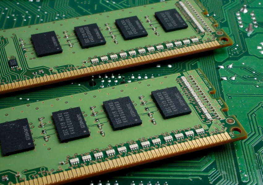
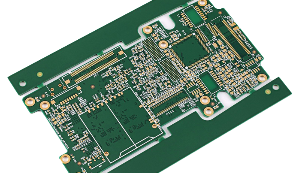
HDI (High Density Interconnect) PCBs refer to printed circuit boards with a higher wiring density than traditional PCBs. They allow for tighter spacing and thinner traces, enabling more compact and complex circuit designs. There are several types of HDI PCBs, categorized by the number of layers, density, and manufacturing process.
Layer Types
2-Layer HDI
Two-layer HDI boards have the following characteristics:
- Trace/space: 3/3 mil (0.0762 mm) or less
- Via pad size: 4-6 mil
- Microvia: Yes (2-3 mil drill)
- High-performance materials: Yes
They are the simplest type of HDI PCB with only 2 conductor layers. The tight trace spacing and microvias enable high interconnect density.
4-Layer HDI
Four-layer HDI boards have the following specifications:
- Trace/space: 2/2 mil (0.0508 mm) or less
- Via pad size: 4-5 mil
- Microvia: Yes (1-2 mil drill)
- High-performance materials: Yes
The additional internal planes provide better electrical performance over 2-layer HDI but are more complex to manufacture.
6+ Layer HDI
Multilayer HDI boards with 6 or more layers allow for further miniaturization and performance. Key characteristics:
- Trace/space: 1/1 mil (0.0254 mm) or less
- Microvia: Yes (0.5-1 mil drill)
- Buried and blind vias
- Very complex to manufacture
They integrate multiple fine-line layers and laser-drilled microvias for high interconnect density. Used in advanced products like smartphones.
Stacked Microvia HDI
This type uses stacked or staggered microvias to connect multiple layers. Allows routing in tight spaces by stacking vias to reach inner layers.
Any-Layer HDI
Any-Layer HDI boards have microvias that can connect any two layers rather than just adjacent layers. Provides design flexibility but requires advanced manufacturing capability.
Density Types
3/3 HDI
Refers to trace/space of 3/3 mil. A common level of HDI technology.
2/2 HDI
Denser trace/space of 2/2 mil. Used in more advanced designs.
1/1 HDI
The densest trace/space of 1/1 mil. Reserved for the most advanced applications. Requires specialized materials and processes.
Manufacturing Process Types
Subtractive HDI
Uses a subtractive process where copper is etched away to form the circuitry. Limited in terms of achievable density.
Semi-Additive HDI
Uses a semi-additive process with electroplating to build up the traces. Enables finer features than subtractive.
Fully Additive HDI
Traces are additively plated without etching. Allows for the densest routing down to 1/1 mil lines. But more complex process.
Modified Semi-Additive Process (MSAP) HDI
A hybrid process combining semi-additive electroplating on an etched thin copper surface. Combines benefits of subtractive and semi-additive.
Any-Layer HDI Manufacturing
Uses advanced drills and plating to produce any-layer microvias. Extremely complex process requiring the latest equipment.
Typical Applications
- Smartphones
- Tablets/Laptops
- Wearable devices
- High-speed digital circuits
- Portable medical devices
- Advanced military/aerospace systems
HDI allows fitting more functions into smaller products. The higher cost is warranted for advanced consumer gadgets, digital systems, and mission-critical applications.
Pros and Cons of HDI PCBs

Pros
- Smaller size and weight
- Increased component density
- Improved electrical performance
- Higher speed signals
- More routing channels
- Complex circuit capabilities
- Miniaturization
Cons
- Increased cost
- Challenging design/assembly
- Specialized manufacturing equipment required
- Limited board sizes
- Testing difficulties
- Thermal management issues
Frequently Asked Questions
What are some key differences between HDI and conventional PCBs?
Some key differences are:
- Much smaller trace/space enables higher wiring density
- Use of microvias vs standard vias
- More layers allow routing between layers
- High-performance materials handle faster signal speeds
- Tighter tolerances required in fabrication
- More complex and expensive manufacturing process
Why can’t standard PCB manufacturing be used for HDI boards?
Standard PCB processes cannot achieve the tight features and tolerances needed for HDI. HDI requires specialized techniques like laser drilling, fine line lithography, and advanced metal deposition. The high density also requires superior materials.
What design considerations are important for HDI PCB layout?
Critical HDI layout considerations include:
- Accounting for tighter routing spacing
- Minimizing unnecessary vias
- Allowing adequate escape routing from BGAs/chips
- Managing layer stackup and lamination thickness
- Controlling impedance for high-speed traces
- Thermal management of layers
- Minimizing stubs
Can component assembly be automated for HDI PCBs?
Assembly can be automated, but HDI typically requires more advanced SMT equipment to handle the high density and small components used. Fine pitch ICs, 01005 passives, microBGAs, and other microcomponents demand specialized pick-and-place machines.
How is HDI PCB testing different from regular PCBs?
HDI testing requires advanced techniques like flying probe, automated xray inspection (AXI), and boundary scan. Dense boards are difficult to fixture and probe. Functional testing at high speeds can also be challenging. Impedance, signal integrity, and EMI must be verified.
Conclusion
HDI PCB technology enables greater miniaturization, performance, and functionality through high wiring density. It comes at a higher cost but is vital for products demanding advanced circuitry in compact form factors. HDI continues advancing as fabrication methods and materials improve. Understanding the various HDI types and tradeoffs helps in designing and applying this key technology.


Leave a Reply