Introduction to solder mask and paste mask
In the world of printed circuit board (PCB) manufacturing, solder mask and paste mask are two important materials used in the production process. While they may sound similar, they serve different purposes and have distinct characteristics. Understanding the differences between solder mask and paste mask is crucial for anyone involved in PCB design and fabrication.
What is solder mask?
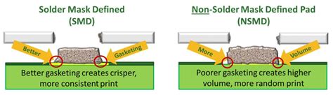
Solder mask, also known as solder resist or solder stop mask, is a thin layer of polymer that is applied to the copper traces of a PCB. Its primary purpose is to protect the copper from oxidation and prevent solder bridges from forming between adjacent pads during the soldering process. Solder mask also provides electrical insulation and helps to improve the aesthetics of the PCB by giving it a uniform color, typically green or blue.
What is paste mask?
Paste mask, on the other hand, is a stencil-like material used to apply solder paste onto the PCB pads prior to component placement. It is typically made of stainless steel or polyimide and contains laser-cut openings that correspond to the pads on the PCB. The paste mask ensures that the correct amount of solder paste is deposited on each pad, which is crucial for achieving reliable solder joints during the reflow soldering process.
Key differences between solder mask and paste mask
While both solder mask and paste mask are essential in the PCB manufacturing process, they have several key differences:
Purpose
- Solder mask: Protects the copper traces, provides insulation, and prevents solder bridges.
- Paste mask: Applies solder paste onto the PCB pads for component placement.
Material
- Solder mask: Typically a polymer, such as epoxy or acrylic.
- Paste mask: Usually made of stainless steel or polyimide.
Application method
- Solder mask: Applied using screen printing, photoimaging, or liquid photoimageable (LPI) processes.
- Paste mask: Used as a stencil to deposit solder paste onto the PCB pads.
Thickness
- Solder mask: Typically 0.5 to 2 mils (0.0127 to 0.0508 mm) thick.
- Paste mask: Usually 4 to 8 mils (0.1016 to 0.2032 mm) thick, depending on the component and pad sizes.
Color
- Solder mask: Commonly green or blue, but can also be red, yellow, black, or white.
- Paste mask: Not applicable, as it is a stencil and does not remain on the PCB after solder paste application.

Solder mask types and properties
There are several types of solder mask available, each with its own set of properties and advantages:
Liquid photoimageable (LPI) solder mask
LPI solder mask is the most common type used in PCB manufacturing. It is applied as a liquid and then exposed to UV light through a photomask, which hardens the exposed areas. The unexposed areas are then removed using a developer solution, leaving the desired solder mask pattern on the PCB.
Advantages of LPI solder mask:
– High resolution and accuracy
– Excellent adhesion to the PCB surface
– Good electrical insulation properties
– Resistant to solvents and high temperatures
Dry film solder mask
Dry film solder mask is a solid film that is laminated onto the PCB surface using heat and pressure. It is then exposed to UV light through a photomask and developed, similar to the LPI process.
Advantages of dry film solder mask:
– Faster application process compared to LPI
– More cost-effective for high-volume production
– Good electrical insulation properties
– Resistant to solvents and high temperatures
Peelable solder mask
Peelable solder mask is a temporary mask that is applied to the PCB to protect certain areas during the soldering process. After soldering, the mask can be easily peeled off, leaving the protected areas clean and free of solder.
Advantages of peelable solder mask:
– Allows for selective soldering of components
– Protects sensitive areas from solder and flux
– Easy to remove after soldering
– Cost-effective for low-volume or prototype production

Paste mask characteristics and considerations
When selecting a paste mask for your PCB manufacturing process, there are several factors to consider:
Material
Stainless steel and polyimide are the most common materials used for paste masks. Stainless steel is more durable and can be used for higher-volume production, while polyimide is more flexible and better suited for fine-pitch components and smaller pad sizes.
Thickness
The thickness of the paste mask determines the amount of solder paste deposited on the PCB pads. Thicker masks are used for larger components and pads, while thinner masks are better for smaller components and fine-pitch applications. Common paste mask thicknesses range from 4 to 8 mils (0.1016 to 0.2032 mm).
Aperture size and shape
The aperture size and shape of the paste mask openings should match the size and shape of the PCB pads. This ensures that the correct amount of solder paste is deposited on each pad, which is crucial for achieving reliable solder joints. Aperture sizes are typically 1:1 with the pad size, but can be adjusted based on the specific requirements of the PCB design.
Alignment and registration
Proper alignment and registration of the paste mask to the PCB is critical for accurate solder paste deposition. Misalignment can result in insufficient or excessive solder paste on the pads, leading to poor solder joint quality or even component failure. Many paste mask suppliers offer fiducial marks or alignment features to help ensure accurate registration during the solder paste printing process.

FAQ
1. Can solder mask and paste mask be used together on the same PCB?
Yes, solder mask and paste mask are used together in the PCB manufacturing process. Solder mask is applied to the PCB first to protect the copper traces and provide insulation. Paste mask is then used to apply solder paste onto the exposed pads prior to component placement and soldering.
2. What is the typical solder mask thickness for a PCB?
The typical solder mask thickness ranges from 0.5 to 2 mils (0.0127 to 0.0508 mm). The specific thickness depends on the PCB design requirements, such as the component sizes, pad spacing, and electrical insulation needs.
3. Can solder mask color affect the performance of the PCB?
The color of the solder mask does not directly affect the electrical performance of the PCB. However, some colors may be better suited for certain applications. For example, black solder mask is often used in high-end audio equipment to minimize light reflection, while white solder mask can improve the contrast for visual inspection and labeling.
4. How often should a paste mask be replaced?
The lifespan of a paste mask depends on several factors, such as the material, usage frequency, and cleaning practices. Stainless steel paste masks can typically last for several thousand prints, while polyimide masks may need to be replaced more frequently. It is important to regularly inspect the paste mask for signs of wear, damage, or clogging, and replace it as necessary to ensure consistent solder paste deposition quality.
5. Can a PCB be manufactured without solder mask?
While it is possible to manufacture a PCB without solder mask, it is not recommended for most applications. Solder mask provides important benefits, such as protecting the copper traces from oxidation, preventing solder bridges, and providing electrical insulation. PCBs without solder mask are more susceptible to damage, contamination, and short circuits, which can lead to reduced reliability and performance. However, in some specific cases, such as high-frequency RF circuits or certain prototyping scenarios, a PCB without solder mask may be appropriate.
Conclusion
Solder mask and paste mask are two essential materials used in the PCB manufacturing process, each serving a distinct purpose. Solder mask protects the copper traces, provides insulation, and prevents solder bridges, while paste mask is used to apply solder paste onto the PCB pads for component placement and soldering.
Understanding the differences between solder mask and paste mask, as well as their types, properties, and characteristics, is crucial for anyone involved in PCB design and fabrication. By selecting the appropriate solder mask and paste mask for your specific application and ensuring proper alignment and registration during the manufacturing process, you can achieve high-quality, reliable PCBs that meet your design requirements.
As PCB technology continues to advance, with smaller components, higher densities, and more complex designs, the importance of solder mask and paste mask will only continue to grow. By staying informed about the latest developments and best practices in PCB manufacturing, you can ensure that your products remain at the forefront of innovation and performance.
Comparison table: Solder mask vs. Paste mask
| Feature | Solder Mask | Paste Mask |
|---|---|---|
| Purpose | Protects copper traces, provides insulation, prevents solder bridges | Applies solder paste onto PCB pads |
| Material | Polymer (epoxy, acrylic) | Stainless steel, polyimide |
| Application Method | Screen printing, photoimaging, liquid photoimageable (LPI) | Stencil for solder paste deposition |
| Thickness | 0.5 to 2 mils (0.0127 to 0.0508 mm) | 4 to 8 mils (0.1016 to 0.2032 mm) |
| Color | Green, blue, red, yellow, black, white | Not applicable (stencil) |


Leave a Reply