Introduction to Tented Vias
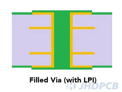
Tented vias are a type of via structure used in printed circuit board (PCB) design and manufacturing. Vias are small holes drilled through a PCB that allow electrical connections between different layers of the board. In the case of tented vias, these holes are covered or “tented” with solder mask on one or both sides of the board, leaving a small opening for electrical connectivity.
Types of Vias
There are several types of vias used in PCB design:
- Through-hole vias
- Blind vias
- Buried vias
- Microvias
- Tented vias
Each type of via serves a specific purpose and has its own advantages and disadvantages.
Advantages of Tented Vias
Tented vias offer several benefits in PCB design and manufacturing:
1. Improved Reliability
By covering the via holes with solder mask, tented vias provide an extra layer of protection against environmental factors such as moisture, dust, and contaminants. This helps to improve the overall reliability of the PCB, especially in harsh environments.
2. Enhanced Mechanical Strength
Tenting the vias with solder mask adds mechanical strength to the PCB structure. This is particularly important for boards that undergo frequent handling or are subject to vibrations and shocks.
3. Reduced Solder wicking
During the soldering process, solder can sometimes flow into the via holes, causing a phenomenon known as solder wicking. Tented vias help to prevent this by limiting the amount of exposed metal in the via, thus reducing the likelihood of solder wicking.
4. Improved High-Frequency Performance
Tented vias can help to improve the high-frequency performance of a PCB by reducing the amount of exposed metal in the via. This helps to minimize signal reflections and other high-frequency signal integrity issues.
Disadvantages of Tented Vias
While tented vias offer several benefits, there are also some potential drawbacks to consider:
1. Increased Manufacturing Complexity
Tenting Vias adds an extra step to the PCB manufacturing process, which can increase the overall complexity and cost of production. This is particularly true for designs that require a large number of tented vias.
2. Potential for Trapped Gases
During the soldering process, gases can sometimes become trapped within the tented via structure. If not properly vented, these trapped gases can cause reliability issues over time.
3. Limited Visual Inspection
Because the via holes are covered with solder mask, it can be more difficult to visually inspect the quality of the via connections during manufacturing. This can potentially lead to undetected defects or quality issues.

Designing with Tented Vias
When designing a PCB with tented vias, there are several key considerations to keep in mind:
1. Via Size and Spacing
The size and spacing of the vias should be carefully considered to ensure proper electrical connectivity and manufacturability. The specific requirements will depend on the PCB design rules and the capabilities of the manufacturing process.
2. Solder Mask Clearance
It is important to provide adequate clearance between the via and the surrounding solder mask to ensure proper tenting and to avoid any potential manufacturing issues.
3. Via Placement
The placement of tented vias should be carefully considered to minimize the impact on signal integrity and to ensure proper manufacturability. Vias should be placed away from critical signal traces and should be distributed evenly across the board to minimize stress and warpage.
Manufacturing Tented Vias
The manufacturing process for tented vias typically involves the following steps:
- Drilling the via holes
- Plating the via holes with copper
- Applying solder mask over the via holes
- Exposing and developing the solder mask to create the tented via structure
- Finishing the PCB with surface treatments such as HASL, ENIG, or OSP
It is important to work closely with the PCB manufacturer to ensure that the tented via design can be properly manufactured and to address any potential issues or concerns.
Tented Via Design Rules
When designing tented vias, there are several key design rules to follow:
| Parameter | Minimum | Recommended |
|---|---|---|
| Via Diameter | 0.2mm | 0.3mm |
| Via Pad Diameter | 0.4mm | 0.5mm |
| Solder Mask Opening | 0.1mm | 0.15mm |
| Solder Mask Clearance | 0.05mm | 0.1mm |
These design rules are intended to ensure proper manufacturability and reliability of the tented via structure. However, the specific requirements may vary depending on the PCB manufacturer and the specific design requirements.
Tented Vias in High-Density PCB Designs
Tented vias are particularly useful in high-density PCB designs where space is limited and signal integrity is critical. By using tented vias, designers can minimize the amount of exposed metal in the via structure, which helps to reduce signal reflections and other high-frequency signal integrity issues.
In high-density designs, it is also important to carefully consider the placement and routing of tented vias to minimize the impact on signal integrity. Tented vias should be placed away from critical signal traces and should be distributed evenly across the board to minimize stress and warpage.
Tented Vias in Flexible PCB Designs
Tented vias are also commonly used in flexible PCB designs, where the board is designed to bend and flex during use. In these applications, tented vias help to improve the mechanical strength and reliability of the via structure, which is critical for ensuring the long-term reliability of the flexible PCB.
When designing tented vias for flexible PCBs, it is important to carefully consider the placement and orientation of the vias to minimize stress and strain on the via structure during flexing. Tented vias should be placed in areas of the board that experience minimal flexing, and should be oriented perpendicular to the direction of flexing to minimize stress.
Testing and Inspection of Tented Vias
Testing and inspection of tented vias is critical for ensuring the quality and reliability of the PCB. There are several methods for testing and inspecting tented vias, including:
- Visual inspection
- X-ray inspection
- Microsectioning
- Electrical testing
Visual inspection is typically used to check for any obvious defects or issues with the tented via structure, such as incomplete tenting or Solder mask damage. X-ray inspection can be used to check for any internal defects or voids in the via structure, while microsectioning involves cross-sectioning the via to inspect the internal structure and plating quality.
Electrical testing is used to verify the electrical connectivity and performance of the tented via structure. This can include resistance testing, impedance testing, and high-frequency signal integrity testing.
Conclusion
Tented vias are a useful via structure for improving the reliability, mechanical strength, and high-frequency performance of PCBs. By covering the via holes with solder mask, tented vias provide an extra layer of protection against environmental factors and help to reduce solder wicking and signal integrity issues.
When designing with tented vias, it is important to carefully consider the size, spacing, and placement of the vias, as well as the specific design rules and manufacturing requirements. Testing and inspection of tented vias is also critical for ensuring the quality and reliability of the PCB.
Overall, tented vias are a valuable tool for PCB designers and manufacturers, offering a range of benefits and advantages for a variety of applications and industries.
FAQ
-
What is the purpose of tented vias in PCB design?
Tented vias serve several purposes in PCB design, including improving reliability, enhancing mechanical strength, reducing solder wicking, and improving high-frequency performance. -
What are the different types of vias used in PCB design?
The different types of vias used in PCB design include through-hole vias, blind vias, buried vias, microvias, and tented vias. Each type of via serves a specific purpose and has its own advantages and disadvantages. -
What are the potential drawbacks of using tented vias?
Some potential drawbacks of using tented vias include increased manufacturing complexity, potential for trapped gases, and limited visual inspection capabilities. -
What are the key design considerations when using tented vias?
When designing with tented vias, it is important to carefully consider the via size and spacing, solder mask clearance, and via placement to ensure proper manufacturability and signal integrity. -
How are tented vias manufactured?
The manufacturing process for tented vias typically involves drilling the via holes, plating the via holes with copper, applying solder mask over the via holes, exposing and developing the solder mask to create the tented via structure, and finishing the PCB with surface treatments such as HASL, ENIG, or OSP.
Leave a Reply