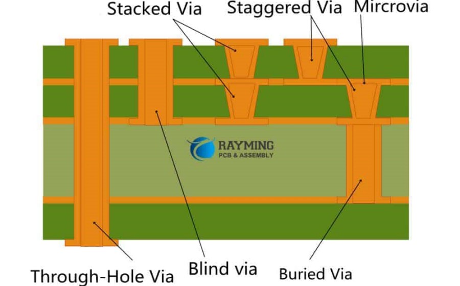
Vias are conductive holes in a printed circuit board (PCB) that allow connections between different layers. There are a few different types of vias:
Normal Vias
Normal vias are the most common type of via used in PCBs. They connect two or more layers vertically by forming a conductive path through the entire board.
Features:
- Connect two or more layers
- Go through entire board vertically
- Often plated with copper for conductivity
- Allow components on different layers to connect
Uses:
- Creating connections between layers for traces
- Connecting surface mount components to inner layer traces
- Providing accessibility for testing points
Normal vias are the standard via used in multilayer PCBs. They form straight vertical connections from the top layer through the entire board to the bottom layer. Normal vias are plated with copper to provide conductivity between the layers.
Blind Vias

Blind vias connect an outer layer of a PCB to one or more inner layers but do not go through the entire board vertically. They are called “blind” because they stop at an internal layer and don’t reach the other side of the board.
Features:
- Connect an outer layer to one or more inner layers
- Do not go through the entire board
- Often plated with copper for conductivity
- Allow connections between outer and inner layers
Uses:
- Connecting surface mount components to inner traces
- Creating connections between outer and inner layers
- Used when connections are not needed through the entire board
Blind vias stop at an internal layer instead of passing vertically through the whole board. This allows connections between the outer and inner layers without using up vertical space through the entire board. Blind vias are commonly used when building up complex, dense boards.
Buried Vias
Buried vias connect two or more internal layers of a PCB without connecting to either outer layer. They are “buried” inside the board between the inner layers.
Features:
- Connect two or more internal layers
- Do not connect to either outer layer
- Often plated with copper for conductivity
- Allow inner layer-to-layer connections
Uses:
- Creating connections between internal layers for traces
- Connecting components located on inner layers
- Providing accessibility for inner layer testing points
Buried vias provide connections only between the internal layers, allowing routing between inner layer components and traces without using up space on the outer layers. Buried vias help optimize signal and component density in complex multi-layer boards.
Comparison Between Via Types
| Via Type | Description |
|---|---|
| Normal | Connect two or more layers vertically through entire board |
| Blind | Connect outer layer to one or more inner layers, don’t pass through entire board |
| Buried | Connect two or more inner layers, don’t connect to either outer layer |
When to use each:
- Use normal vias when you need direct vertical connections through the entire board
- Use blind vias when you only need to connect an outer and inner layer, saving space
- Use buried vias when you just need inner layer-to-layer connections
Fabrication:
- Normal vias are simplest to fabricate, just drilling through each layer
- Blind vias require precise depth control when drilling to stop at the middle layer
- Buried vias have additional steps to fill prior layers before drilling the buried hole
Routing:
- Normal vias take up vertical routing space through whole board
- Blind/buried vias don’t consume vertical space since they stop at internal layers
- Blind/buried vias allow for denser boards by only using necessary layers
Advantages of Blind and Buried Vias
Blind and buried vias offer some key advantages compared to traditional normal vias:
More routing space:
- Blind/buried vias don’t have to pass through every layer, saving vertical routing space
- This allows for more trace routing flexibility on the outer layers
Higher density:
- Stacking components on internal layers is possible without occupying outer layer space
- Allows for more compact component placement and denser designs
Reduce layer count:
- Using blind/buried vias can eliminate the need for additional layers
- Functions requiring dedicated layers can be integrated internally using blind/buried vias
Improve signal integrity:
- Critical signals can be routed internally with blind/buried vias
- This shields signals from noise interference compared to external routing
Enable buried component placement:
- Components can be placed internally and connected with blind/buried vias
- Saves space compared to placing components on outer layers
Reduce manufacturing costs:
- Using fewer layers by leveraging blind/buried vias reduces fabrication costs
- May also reduce drilling/imaging time depending on design
Blind and buried vias enable more efficient use of layers and space in complex PCB designs. They are critical for modern high-density PCBs.
Disadvantages of Blind and Buried Vias
Despite their advantages, blind and buried vias also come with some downsides:
Increased fabrication complexity:
- Controlling blind via depth and filling prior layers for buried vias is more complex
- This can increase the risk of defects during manufacturing
More difficult rework and repair:
- It’s harder to access blind/buried vias for rework compared to normal vias
- Specialized micro-drills may be needed to reach buried and blind vias
Requires advanced PCB fab capabilities:
- Not all manufacturers support advanced processes for blind/buried vias
- Especially true for inexpensive and/or low volume fabrication options
Higher fabrication costs:
- The additional process steps increase costs compared to standard vias
- Blind/buried vias work best for larger volume production runs
Challenging design and layout:
- Routing and layout with blind/buried vias requires more planning
- Must carefully track vertical alignments between layers
Not suitable for some applications:
- If connections are needed through the full board, blind/buried vias won’t work
- Normal vias should still be used in some cases
The specialized nature of blind and buried vias makes them most feasible for companies producing large volumes of complex, multilayer boards. They require proper design, layout, and manufacturer capabilities.
Key Considerations When Using Blind and Buried Vias
Here are some important factors to consider when working with blind and buried vias in your PCB design:
Choose the right manufacturer
Make sure your board fab shop can support the specialized processes required for blind and buried vias – not all can. Share your layer stackup and via plans early.
Follow manufacturer design rules
Different manufacturers have specific design rules for blind and buried vias including size, spacing, annular rings, etc. Follow their guidelines.
Plan layer transitions carefully
Think through all your vertical layer transition needs upfront. Map out whereblind/buried vias are needed to route between layers.
Account for via-in-pad designs
If your design requires blind/buried vias to be covered under component pads, inform your manufacturer early as this affects fabrication processes.
Keep high-speed design in mind
Blind and buried vias can help isolate critical traces from noise. Plan your stackup and use them strategically for best SI/PI.
Get your designer CAD tools right
Your PCB design software needs the right capabilities to handle blind/buried vias. Work with your EDA vendor to implement advanced via features.
Perform thorough design rule checks
Leverage your CAD tools to run comprehensive DRC on blind/buried via spacing, annular rings, depth, etc. to catch errors early.
Build and review prototypes
Validate blind and buried via implementation with initial prototype runs. Examine cross-sections under a microscope if needed to check quality.
Adjust designs based on feedback
If prototypes reveal issues with certain blind or buried vias, make adjustments to your design rules and layouts accordingly.
Leveraging blind and buried vias takes some additional planning and implementation considerations but enables smaller, higher performance PCB designs.
Frequently Asked Questions
What are the key benefits of using blind and buried vias?
The main benefits of using blind and buried vias are increased routing space, higher component density, reduced layer counts, improved signal integrity, and enabling buried component placement. This allows for smaller and higher performing PCB designs.
When should normal vias be used vs. blind or buried vias?
Use normal vias when vertical connectivity is needed through the full board stackup. Use blind and buried vias when connections only need to be made on select inner layers, saving space and cost.
Is there a limit to how many blind and buried vias can be used on a PCB?
There are no inherent limits. However, at very high densities of blind/buried vias, fabricating the PCB becomes more difficult and expensive. Consult your manufacturer on any density recommendations.
Can microvias be combined with buried and blind vias?
Yes, microvias (small vias with diameters below 150um) are often paired with buried and blind vias to further increase routing density for complex high density interconnects (HDI) boards.
How do blind and buried vias impact PCB fabrication lead times?
Because of the additional steps required, boards with blind/buried vias typically have higher lead times – often 25% to 50% longer. However, fabrication processes continue improving to reduce this impact.
Can buried and blind vias be implemented without using advanced PCB technology?
It is very challenging. Simple two-layer boards with manual drilling could potentially implement buried vias but traditional fabrication processes won’t support blind vias or more complex buried configurations.
How are defects in buried vias detected and repaired?
X-ray imaging is essential for detecting faults in buried vias. Repairing buried vias can require specialized micro etching techniques. Blind vias are easier to access and repair.
Does it cost more to implement buried and blind vias?
Yes, the specialized fabrication steps required typically result in higher costs compared to standard vias. However, the benefits often justify the costs for complex, high volume designs.
Can buried and blind vias be implemented on flex PCBs?
Yes, photoimageable coverlay materials enable creating openings for blind and buried vias in flex PCBs. This provides flexibility routing benefits while maintaining dynamic flexing performance.


Leave a Reply