Introduction to PCB Fabrication
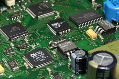
Printed Circuit Board (PCB) fabrication is the process of creating a functional circuit board from a design layout. PCBs are essential components in modern electronics, providing a platform for integrating and connecting various electronic components. Two-layer PCBs are the most basic type of multi-layer PCBs, consisting of two conductive layers separated by an insulating substrate. In this article, we will explore the process of two-layer PCB fabrication in detail.
The Importance of Two Layer PCBs
Two-layer PCBs are widely used in various electronic applications due to their simplicity, cost-effectiveness, and reliability. They offer several advantages over single-layer PCBs, including:
- Increased design flexibility
- Improved signal integrity
- Better power distribution
- Reduced electromagnetic interference (EMI)
These benefits make two-layer PCBs a popular choice for many electronic projects, ranging from simple prototypes to complex industrial applications.

The PCB Fabrication Process
The fabrication of two-layer PCBs involves several critical steps, each contributing to the quality and functionality of the final product. The main steps in the PCB fabrication process are:
- Design and Layout
- PCB Material Selection
- Copper Clad Lamination
- Drilling
- Copper Plating
- Etching
- Solder Mask Application
- Silkscreen Printing
- Surface Finish Application
- Electrical Testing and Inspection
Let’s delve into each of these steps in more detail.
1. Design and Layout
The PCB fabrication process begins with the design and layout of the circuit. This step involves creating a schematic diagram of the electronic circuit and translating it into a physical layout using PCB design software. The layout determines the placement of components, traces, and vias on the PCB.
Key considerations during the design and layout phase include:
- Component footprints and land patterns
- Trace width and spacing
- Via size and placement
- Power and ground plane design
- Signal integrity and EMI reduction techniques
2. PCB Material Selection
The choice of PCB material is crucial for the performance and reliability of the final product. The most common material used for two-layer PCBs is FR-4, a glass-reinforced epoxy laminate. FR-4 offers good mechanical strength, electrical insulation, and thermal stability.
Other factors to consider when selecting PCB material include:
- Dielectric constant and loss tangent
- Thermal conductivity
- Coefficient of thermal expansion (CTE)
- Flammability rating
- Cost and availability
3. Copper Clad Lamination
Once the PCB material is selected, the next step is to laminate a thin layer of copper foil onto both sides of the insulating substrate. This process involves applying heat and pressure to bond the copper foil to the substrate, creating a copper-clad laminate.
The thickness of the copper foil is typically expressed in ounces per square foot (oz/ft²). Common copper weights for two-layer PCBs are 1 oz/ft² and 2 oz/ft².
4. Drilling
After the copper-clad laminate is prepared, holes are drilled through the board to accommodate through-hole components and vias. The drilling process is typically performed using computer numerical control (CNC) machines, which ensure precise hole placement and size.
Key factors to consider during the drilling process include:
- Drill bit size and material
- Hole diameter and tolerance
- Aspect ratio (hole depth to diameter ratio)
- Deburring and cleaning of drilled holes
5. Copper Plating
The drilled holes are then plated with copper to create electrical connections between the top and bottom layers of the PCB. This process is known as electroplating or through-hole plating.
The copper plating process involves the following steps:
- Cleaning and activating the hole walls
- Applying a thin layer of electroless copper
- Electroplating additional copper to achieve the desired thickness
- Planarizing the surface to remove excess copper
6. Etching
The next step in the PCB fabrication process is etching, which removes unwanted copper from the laminate to create the desired circuit pattern. This is typically done using a photolithographic process.
The etching process involves the following steps:
- Applying a photoresist layer to the copper surface
- Exposing the photoresist to UV light through a photomask
- Developing the photoresist to remove the exposed areas
- Etching away the unwanted copper using a chemical etchant
- Stripping the remaining photoresist
The choice of etchant and etching method depends on factors such as the copper thickness, desired etch rate, and environmental considerations.
7. Solder Mask Application
After etching, a solder mask layer is applied to the PCB to protect the copper traces and prevent solder bridging during the assembly process. The solder mask is a thin, protective coating that covers the entire PCB surface, except for the areas where components will be soldered (e.g., pads and vias).
Solder masks are typically applied using a screen printing or photoimaging process, and they are available in various colors, with green being the most common.
8. Silkscreen Printing
Silkscreen printing is used to add text, logos, and other markings to the PCB surface. This step is essential for component identification, assembly instructions, and branding.
The silkscreen printing process involves applying ink through a fine mesh screen onto the PCB surface. The ink is typically white, but other colors are available for special applications.
9. Surface Finish Application
The final step in the PCB fabrication process is the application of a surface finish to the exposed copper areas. The surface finish serves several purposes, including:
- Protecting the copper from oxidation and corrosion
- Enhancing solderability
- Improving electrical conductivity
- Providing a better surface for component assembly
Common surface finishes for two-layer PCBs include:
- Hot Air Solder Leveling (HASL)
- Organic Solderability Preservative (OSP)
- Electroless Nickel Immersion Gold (ENIG)
- Immersion Silver (IAg)
- Immersion Tin (ISn)
The choice of surface finish depends on factors such as the intended application, environmental requirements, and cost.
10. Electrical Testing and Inspection
After the PCB fabrication process is complete, the boards undergo thorough electrical testing and inspection to ensure they meet the required specifications and are free from defects. This step is crucial for guaranteeing the quality and reliability of the final product.
Electrical testing typically involves:
- Continuity testing to verify electrical connections
- Insulation resistance testing to check for shorts and leakage
- High-potential (HiPot) testing to ensure dielectric strength
Visual inspection is also performed to check for physical defects, such as:
- Misaligned or missing holes
- Incomplete or over-etched traces
- Solder mask or silkscreen defects
- Contamination or foreign materials
Automated optical inspection (AOI) systems are often used to streamline the inspection process and detect defects that may be difficult to identify with the naked eye.

Advantages of Two Layer PCB Fabrication
Two-layer PCB fabrication offers several advantages over single-layer PCBs, making them a popular choice for various electronic applications. Some of the key advantages include:
-
Increased Design Flexibility
Two-layer PCBs allow for more complex circuit designs and higher component densities compared to single-layer boards. The additional layer provides more routing options and enables the use of power and ground planes, which can improve signal integrity and reduce electromagnetic interference (EMI). -
Improved Signal Integrity
By using a dedicated ground plane, two-layer PCBs can significantly reduce signal noise and crosstalk. This is particularly important for high-speed digital circuits and sensitive analog applications. -
Better Power Distribution
Two-layer PCBs enable the use of power planes, which provide a low-impedance path for distributing power to components. This can help reduce voltage drops and improve overall power supply stability. -
Enhanced Mechanical Stability
The additional layer in two-layer PCBs provides increased mechanical strength and rigidity compared to single-layer boards. This can help prevent warping and improve the overall durability of the PCB. -
Cost-Effective
While two-layer PCBs are more expensive than single-layer boards, they are still relatively cost-effective compared to multi-layer PCBs with more than two layers. This makes them a good choice for projects that require the benefits of a two-layer design without the added complexity and cost of higher-layer-count boards.

Challenges in Two Layer PCB Fabrication
Despite the many advantages of two-layer PCBs, there are also some challenges associated with their fabrication. These challenges can impact the quality, reliability, and cost of the final product.
Some common challenges in two-layer PCB fabrication include:
-
Dimensional Accuracy
Maintaining tight tolerances and ensuring accurate hole placement can be challenging, especially for high-density designs. Factors such as material expansion and contraction, drill bit wear, and etching process variations can all contribute to dimensional inaccuracies. -
Copper Thickness Variations
Uneven copper thickness across the PCB can lead to impedance mismatches and signal integrity issues. Careful process control is necessary to maintain consistent copper thickness during the plating and etching steps. -
Solder Mask and Silkscreen Registration
Aligning the solder mask and silkscreen layers with the copper traces and pads can be challenging, particularly for fine-pitch components and high-density designs. Misalignment can lead to assembly difficulties and potential reliability issues. -
Trace Width and Spacing Limitations
The minimum trace width and spacing achievable in two-layer PCB fabrication are limited by the capabilities of the etching process and the properties of the PCB material. Pushing these limits can increase the risk of manufacturing defects and signal integrity problems. -
Materials Selection and Compatibility
Choosing the right combination of PCB materials, surface finishes, and solder mask can be complex, as each material has its own properties and compatibility requirements. Incorrect material selection can lead to issues such as delamination, warping, and poor solderability.
Addressing these challenges requires careful design consideration, close collaboration with the PCB fabricator, and adherence to industry standards and best practices.
FAQ
-
What is the typical turnaround time for two-layer PCB fabrication?
The turnaround time for two-layer PCB fabrication can vary depending on the complexity of the design, the quantity ordered, and the capabilities of the fabricator. However, a typical turnaround time for a standard two-layer PCB is between 3 to 5 working days. -
What is the minimum feature size achievable in two-layer PCB fabrication?
The minimum feature size in two-layer PCB fabrication depends on the capabilities of the fabricator and the specific process used. Typically, a minimum trace width and spacing of 4 to 6 mils (0.1 to 0.15 mm) can be achieved. However, some advanced fabricators may be able to achieve even smaller feature sizes. -
Can two-layer PCBs be used for high-frequency applications?
Yes, two-layer PCBs can be used for high-frequency applications, provided that proper design techniques are employed. These techniques include the use of controlled impedance traces, ground planes, and careful component placement to minimize signal integrity issues and EMI. -
What are the most common surface finishes for two-layer PCBs?
The most common surface finishes for two-layer PCBs are Hot Air Solder Leveling (HASL), Organic Solderability Preservative (OSP), and Electroless Nickel Immersion Gold (ENIG). Each surface finish has its own advantages and disadvantages in terms of cost, solderability, and shelf life. -
How can I ensure the quality and reliability of my two-layer PCBs?
To ensure the quality and reliability of your two-layer PCBs, it is essential to work with a reputable PCB fabricator that adheres to industry standards and best practices. Additionally, thorough electrical testing and visual inspection should be performed on the finished boards to identify any potential defects or issues. Following proper design guidelines and considering the specific requirements of your application can also help ensure the quality and reliability of your two-layer PCBs.
| Aspect | Single-layer PCB | Two-layer PCB |
|---|---|---|
| Design Flexibility | Limited | Increased |
| Signal Integrity | Lower | Improved |
| Power Distribution | Basic | Enhanced |
| Mechanical Stability | Lower | Higher |
| Cost | Lower | Moderate |
Conclusion
Two-layer PCB fabrication is a critical process in the production of modern electronic devices. By understanding the various steps involved in the fabrication process, as well as the advantages and challenges associated with two-layer PCBs, designers and engineers can make informed decisions when developing their electronic products.
Proper design techniques, material selection, and close collaboration with experienced PCB fabricators are essential for ensuring the quality, reliability, and cost-effectiveness of two-layer PCBs. As technology continues to advance, the role of two-layer PCBs in the electronics industry is likely to remain significant, providing a balance between performance and affordability for a wide range of applications.


Leave a Reply