What is Through-hole Technology?
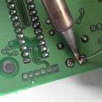
Through-hole technology refers to the method of mounting electronic components on a PCB by inserting their leads through drilled holes and soldering them onto the opposite side of the board. The holes are typically plated with a conductive material, such as copper, to establish electrical connections between the component leads and the PCB traces.
Types of Through-hole Components
Through-hole components come in various packages, each with its own set of characteristics and applications. Some common types include:
- Dual In-line Package (DIP): DIPs are widely used for integrated circuits (ICs) and have two parallel rows of leads.
- Single In-line Package (SIP): SIPs have a single row of leads and are often used for resistor networks and connectors.
- Radial Lead: Radial lead components, such as capacitors and inductors, have leads extending from one side of the component body.
- Axial Lead: Axial lead components, such as resistors and diodes, have leads extending from opposite ends of the component body.
Advantages of Through-hole PCBs
Through-hole PCBs offer several advantages that make them suitable for various applications:
Mechanical Stability
Through-hole components are mechanically secured to the PCB by their leads, which are soldered onto the board. This provides a strong physical connection that can withstand vibration, shock, and thermal stress better than surface-mounted components.
Ease of Assembly
Through-hole components are relatively easy to handle and assemble manually, making them ideal for prototyping, low-volume production, and hobbyist projects. The larger component size and visible leads simplify the soldering process and allow for visual inspection of solder joints.
High Power Handling
Through-hole components generally have higher power handling capabilities compared to their surface-mount counterparts. The larger lead diameter and the ability to dissipate heat through the PCB make them suitable for high-power applications, such as power supplies and motor controllers.
Reliability
The robust mechanical connection and the ability to dissipate heat efficiently contribute to the overall reliability of through-hole PCBs. They are less prone to solder joint failures caused by thermal cycling and mechanical stress, making them a preferred choice for mission-critical applications.
Disadvantages of Through-hole PCBs
Despite their advantages, through-hole PCBs have some limitations:
Larger Footprint
Through-hole components require drilled holes and additional space for lead insertion, resulting in a larger footprint compared to surface-mount components. This limits the component density and miniaturization potential of through-hole PCBs.
Higher Manufacturing Cost
The drilling process and the need for plated through-holes add complexity and cost to the PCB manufacturing process. Additionally, the manual assembly of through-hole components is more time-consuming and labor-intensive compared to the automated placement of surface-mount components.
Limited High-frequency Performance
The longer leads of through-hole components introduce parasitic inductance and capacitance, which can degrade high-frequency performance. This makes through-hole PCBs less suitable for high-speed digital circuits and RF applications.

Through-hole PCB Manufacturing Process
The manufacturing process for through-hole PCBs involves several steps:
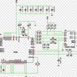
- PCB Design: The PCB layout is designed using computer-aided design (CAD) software, specifying the component placement, drill holes, and trace routing.
- Drilling: Holes are drilled into the PCB substrate using automated drilling machines based on the CAD data.
- Plating: The drilled holes are plated with a conductive material, typically copper, to establish electrical connections between the layers of the PCB.
- Solder Mask Application: A solder mask is applied to the PCB to protect the copper traces and prevent solder bridging during the assembly process.
- Silkscreen Printing: A silkscreen layer is printed onto the PCB to provide component identifiers, labels, and other visual markings.
- Component Placement: Through-hole components are inserted into the drilled holes manually or using automated insertion machines.
- Soldering: The PCB is passed through a wave soldering machine, which applies molten solder to the component leads and PCB pads, forming a strong electrical and mechanical connection.
- Inspection and Testing: The assembled PCB undergoes visual inspection and electrical testing to ensure proper functionality and adherence to quality standards.
Applications of Through-hole PCBs
Through-hole PCBs find applications in various domains:
Industrial Electronics
Industrial control systems, sensors, and actuators often rely on through-hole PCBs due to their robustness and reliability in harsh environments.
Power Electronics
Power supplies, motor controllers, and high-current applications benefit from the high power handling capability and heat dissipation properties of through-hole components.
Automotive Electronics
Through-hole PCBs are used in automotive electronics, such as engine control units (ECUs) and body control modules (BCMs), where reliability and vibration resistance are critical.
Military and Aerospace
Mission-critical systems in military and aerospace applications often employ through-hole PCBs for their reliability and ability to withstand extreme environmental conditions.
Prototyping and Hobbyist Projects
Through-hole PCBs are popular among hobbyists and for prototyping purposes due to their ease of assembly and the availability of through-hole components.
Future of Through-hole Technology
While surface mount technology has become the dominant PCB assembly method, through-hole technology continues to evolve and find its place in modern electronics manufacturing.
Hybrid PCBs
Hybrid PCBs combine through-hole and surface-mount technologies on the same board, leveraging the advantages of both methods. This approach allows for the use of through-hole components for critical or high-power functions while benefiting from the miniaturization and high-density capabilities of surface-mount components.
Advanced Materials
The development of advanced PCB materials, such as high-temperature laminates and low-loss dielectrics, has expanded the capabilities of through-hole PCBs in demanding applications.
Automated Assembly
Advancements in automated through-hole component insertion and soldering technologies have improved the efficiency and reliability of through-hole PCB assembly, making it more viable for high-volume production.
Frequently Asked Questions (FAQ)
1. What is the difference between through-hole and surface-mount technology?
Through-hole technology involves inserting component leads through drilled holes in the PCB and soldering them on the opposite side, while surface-mount technology involves placing components directly onto the surface of the PCB and soldering them in place.
2. Can through-hole and surface-mount components be used on the same PCB?
Yes, hybrid PCBs combine both through-hole and surface-mount components on the same board, allowing designers to leverage the advantages of both technologies.
3. Are through-hole PCBs more expensive than surface-mount PCBs?
Generally, through-hole PCBs are more expensive to manufacture due to the additional drilling and plating processes, as well as the manual assembly of components. Surface-mount PCBs offer cost advantages in high-volume production.
4. What are the advantages of using through-hole components?
Through-hole components offer several advantages, including mechanical stability, ease of assembly, high power handling capability, and reliability in harsh environments.
5. Are through-hole PCBs becoming obsolete?
While surface-mount technology has become the dominant PCB assembly method, through-hole PCBs remain relevant in various applications where their unique advantages are required. Additionally, advancements in materials and automated assembly technologies continue to support the use of through-hole PCBs in modern electronics manufacturing.
Conclusion
Through-hole technology has been a fundamental aspect of PCB fabrication for decades, offering robustness, reliability, and ease of assembly. Despite the widespread adoption of surface-mount technology, through-hole PCBs continue to play a vital role in various applications, particularly in industrial, power, automotive, and mission-critical systems.
As electronics manufacturing evolves, through-hole technology adapts to meet the changing requirements. Hybrid PCBs, advanced materials, and automated assembly technologies are extending the capabilities and relevance of through-hole PCBs in the modern era.
By understanding the advantages, disadvantages, and applications of through-hole technology, designers and manufacturers can make informed decisions when selecting the appropriate PCB fabrication method for their specific needs.
| Aspect | Through-hole PCBs | Surface-mount PCBs |
|---|---|---|
| Component Mounting | Leads inserted through holes | Components placed on surface |
| Mechanical Stability | High | Moderate |
| Component Density | Low | High |
| Power Handling | High | Moderate |
| High-frequency Performance | Limited | Better |
| Manufacturing Cost | Higher | Lower |
| Assembly Method | Manual or automated insertion | Automated placement |
Table 1: Comparison of Through-hole and Surface-mount PCBs
By leveraging the strengths of through-hole technology and combining it with the advantages of surface-mount technology when appropriate, designers and manufacturers can create robust, reliable, and cost-effective PCBs that meet the demands of a wide range of applications.
Leave a Reply