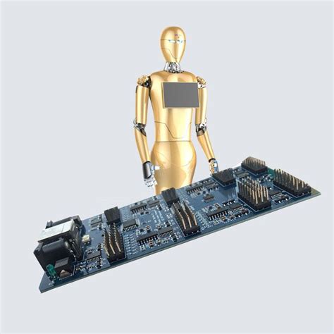
What are PCBs and Why are They Essential in Robotics?
PCBs are thin, flat boards made of insulating material, typically fiberglass or plastic, with conductive copper tracks etched onto their surface. These boards serve as the foundation for mounting and interconnecting electronic components such as microcontrollers, sensors, actuators, and power modules. PCBs provide a compact and organized way to assemble the electronic circuitry required for a robot’s operation.
The importance of PCBs in robotics cannot be overstated. They offer several key benefits:
- Miniaturization: PCBs allow for the dense packaging of electronic components, enabling the creation of compact and lightweight robotic systems.
- Reliability: Well-designed PCBs ensure proper connectivity and minimize the risk of electrical failures, enhancing the reliability of the robot.
- Signal Integrity: PCBs provide controlled impedance and shielding, reducing electromagnetic interference (EMI) and ensuring clean and stable signal transmission.
- Customization: PCBs can be customized to meet the specific requirements of a robotic application, accommodating unique form factors and functionalities.
Types of PCBs Used in Robotics
Robots employ various types of PCBs depending on their complexity and intended use. Some common types include:
- Single-Layer PCBs: These are the simplest and most cost-effective PCBs, with conductive tracks on only one side of the board. They are suitable for basic robotic applications with minimal component density.
- Double-layer PCBs: These PCBs have conductive tracks on both sides of the board, allowing for higher component density and more complex routing. They are widely used in robotics for their increased flexibility and signal routing capabilities.
- Multi-layer PCBs: As the name suggests, these PCBs consist of multiple layers of conductive tracks separated by insulating layers. They offer the highest level of component density and signal routing complexity, making them ideal for advanced robotic systems with numerous sensors, actuators, and processing units.
- Flexible PCBs: These PCBs are made of flexible materials, allowing them to bend and conform to irregular shapes. They are particularly useful in robotics for applications that require flexibility or where space is limited.
Designing PCBs for Robotic Applications
Designing PCBs for robots involves considering various factors to ensure optimal performance, reliability, and functionality. Let’s explore some key aspects of PCB design in robotics.
Schematic Design
The first step in designing a PCB for a robot is creating a schematic diagram. The schematic captures the electrical connections and components required for the robot’s functionality. It serves as a blueprint for the PCB layout and helps in identifying potential issues early in the design process.
When designing the schematic, engineers must consider the following:
- Component selection: Choosing the right components based on their specifications, power requirements, and compatibility with the overall system.
- Power distribution: Ensuring proper power supply to all components, considering voltage levels, current draw, and power sequencing.
- Signal integrity: Minimizing cross-talk, noise, and interference by properly routing signals and implementing necessary filtering and shielding techniques.
PCB Layout
Once the schematic is finalized, the next step is to create the PCB layout. The layout determines the physical placement of components and the routing of conductive tracks on the PCB. Proper layout design is crucial for ensuring signal integrity, minimizing EMI, and facilitating manufacturability.
Key considerations in PCB layout design for robotics include:
- Component placement: Arranging components in a logical and space-efficient manner, taking into account heat dissipation, mechanical constraints, and signal flow.
- Trace routing: Routing the conductive tracks to minimize signal interference, ensure proper impedance control, and avoid crossing sensitive signals.
- Grounding and shielding: Implementing proper grounding strategies and shielding techniques to reduce EMI and maintain signal integrity.
- Manufacturability: Adhering to manufacturing guidelines, such as minimum trace width, spacing, and hole sizes, to ensure the PCB can be reliably produced.
Simulation and Testing
Before sending the PCB for fabrication, it is essential to simulate and test the design to identify and rectify any potential issues. Simulation tools allow engineers to analyze signal integrity, power distribution, and thermal behavior of the PCB.
Additionally, prototyping and testing the PCB with the actual components provide valuable insights into its real-world performance. This stage helps in identifying any design flaws, component incompatibilities, or unexpected behavior, allowing for necessary revisions before mass production.

Advancements in PCB Technology for Robotics
The field of PCB technology is constantly evolving, driven by the growing demands of robotic applications. Some notable advancements include:
- High-Density Interconnect (HDI) PCBs: HDI PCBs offer higher component density and finer trace widths, enabling the integration of more functionality in smaller form factors. They are particularly useful in miniaturized robotic systems.
- Embedded Components: Embedding passive components, such as resistors and capacitors, within the PCB Layers reduces the overall footprint and improves signal integrity. This technique is gaining traction in robotic applications where space is at a premium.
- Flexible and Stretchable PCBs: Advances in materials science have led to the development of flexible and stretchable PCBs that can conform to complex shapes and withstand mechanical stress. These PCBs find applications in wearable robotics and soft robotics.
- 3D PCBs: Three-dimensional PCBs, also known as multi-layer molded interconnect devices (3D-MID), allow for the integration of electronic components in three-dimensional structures. They offer unique design possibilities for robotic systems with intricate geometries.

FAQs
-
What is the difference between a single-layer and a multi-layer PCB in robotics?
A single-layer PCB has conductive tracks on only one side of the board, while a multi-layer PCB consists of multiple layers of conductive tracks separated by insulating layers. Multi-layer PCBs offer higher component density and more complex signal routing capabilities, making them suitable for advanced robotic systems. -
How do I choose the right components for my robot’s PCB?
When selecting components for your robot’s PCB, consider factors such as their specifications, power requirements, and compatibility with the overall system. It’s essential to choose components that meet the performance demands of your robotic application while ensuring proper power distribution and signal integrity. -
What are some common challenges in designing PCBs for robotics?
Some common challenges in PCB design for robotics include managing signal integrity, minimizing electromagnetic interference (EMI), ensuring proper power distribution, and dealing with mechanical constraints. Careful consideration of component placement, trace routing, grounding, and shielding techniques is necessary to overcome these challenges. -
How can I ensure the reliability of my robot’s PCB?
To ensure the reliability of your robot’s PCB, follow best practices in design, such as proper component selection, signal integrity management, and adherence to manufacturing guidelines. Thorough simulation, prototyping, and testing are crucial to identify and rectify any potential issues before mass production. -
What are some emerging trends in PCB technology for robotics?
Some emerging trends in PCB technology for robotics include the use of high-density interconnect (HDI) PCBs for miniaturization, embedded components for space savings, flexible and stretchable PCBs for wearable and soft robotics, and 3D PCBs for integrating electronics in complex geometries.

Conclusion
PCBs form the core of our robotic systems, enabling the integration of electronic components and facilitating the flow of electrical signals. Understanding the significance of PCBs in robotics and the considerations involved in their design is crucial for developing reliable and high-performance robotic systems.
As the field of robotics continues to advance, so does PCB technology. Innovations such as HDI PCBs, embedded components, flexible and stretchable PCBs, and 3D PCBs are reshaping the way we design and build robots. By staying up-to-date with these advancements and applying best practices in PCB design, engineers can create robots that push the boundaries of functionality, efficiency, and reliability.
In conclusion, PCBs play a vital role in bringing our robotic creations to life. As we continue to explore new frontiers in robotics, the importance of well-designed and innovative PCBs will only continue to grow. By understanding and leveraging the power of PCBs, we can build robots that are smarter, faster, and more capable than ever before.
[Word count: 1553 words]


Leave a Reply