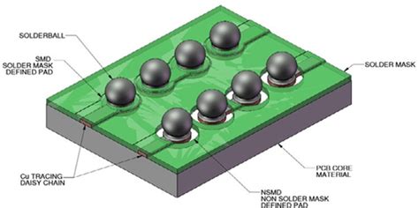
What is LPI Soldermask?
LPI soldermask is a photopolymer coating applied to the surface of a PCB to protect the copper traces and prevent solder bridging during the assembly process. It is a liquid photoimageable material that is sensitive to UV light, allowing for precise patterning and curing. LPI soldermask offers several benefits, including:
- Protection of copper traces from oxidation and damage
- Prevention of solder bridging during assembly
- Electrical insulation between conductive parts
- Improved aesthetics of the final PCB product
Advantages of Silk Screen Printing for LPI Soldermask Application
Silk screen printing has been the go-to method for applying LPI soldermask in the PCB industry for several reasons:
Cost-effectiveness
Compared to other methods like spray coating or curtain coating, silk screen printing is a relatively inexpensive process. It requires minimal equipment and materials, making it an economical choice for PCB manufacturers.
High throughput
Silk screen printing allows for the simultaneous processing of multiple PCBs, enabling high-volume production. This is particularly advantageous for large-scale PCB manufacturing facilities.
Consistency and repeatability
With proper setup and process control, silk screen printing ensures consistent and repeatable LPI soldermask application. This is crucial for maintaining the quality and reliability of the final PCB product.
Versatility
Silk screen printing can be used for a wide range of PCB designs and sizes, making it a versatile choice for various applications.

The LPI Soldermask Silk Screen Printing Process
The silk screen printing process for LPI soldermask application involves several steps:
-
Screen preparation: A fine mesh screen is coated with a light-sensitive emulsion and exposed to a film positive of the desired soldermask pattern. The unexposed areas of the emulsion are then washed away, creating a stencil for the soldermask application.
-
Soldermask application: The LPI soldermask is applied to the PCB surface through the screen using a squeegee. The squeegee forces the soldermask through the open areas of the screen onto the PCB.
-
Pre-drying: After application, the PCB is pre-dried to remove the solvent from the soldermask and prevent it from flowing or smearing.
-
Exposure: The PCB is exposed to UV light, which causes the soldermask to crosslink and harden in the exposed areas.
-
Developing: The unexposed areas of the soldermask are removed using a developer solution, revealing the desired pattern.
-
Curing: The PCB undergoes a final curing process, typically in an oven, to fully harden the soldermask and ensure its adhesion to the PCB surface.
| Step | Description |
|---|---|
| Screen preparation | Create a stencil for soldermask application |
| Soldermask application | Apply LPI soldermask through the screen |
| Pre-drying | Remove solvent and prevent smearing |
| Exposure | Crosslink and harden exposed areas |
| Developing | Remove unexposed areas |
| Curing | Fully harden the soldermask |

Factors Affecting LPI Soldermask Silk Screen Printing Quality
Several factors can influence the quality of LPI soldermask application using silk screen printing:
Screen mesh count and emulsion thickness
The screen mesh count and emulsion thickness determine the resolution and thickness of the applied soldermask. A higher mesh count and thinner emulsion result in finer details and thinner soldermask layers.
Squeegee pressure and speed
The pressure and speed of the squeegee during soldermask application affect the uniformity and thickness of the coating. Consistent pressure and speed are essential for achieving a high-quality finish.
Soldermask viscosity and rheology
The viscosity and rheology of the LPI soldermask play a crucial role in its flow and leveling properties during application. Proper formulation and control of these properties are necessary for optimal results.
Drying and curing conditions
The drying and curing conditions, such as temperature, humidity, and UV exposure, impact the final properties and adhesion of the soldermask. Careful monitoring and control of these parameters are essential for ensuring a reliable and durable soldermask layer.

Frequently Asked Questions (FAQ)
-
Q: What is the typical thickness of LPI soldermask applied using silk screen printing?
A: The typical thickness of LPI soldermask applied using silk screen printing ranges from 0.5 to 1.5 mils (12.7 to 38.1 microns), depending on the screen mesh count and emulsion thickness used. -
Q: Can silk screen printing be used for applying soldermask on both sides of a PCB?
A: Yes, silk screen printing can be used for applying soldermask on both sides of a PCB. This is typically done in two separate passes, with the PCB being flipped over after the first side is processed. -
Q: How does the choice of LPI soldermask material affect the silk screen printing process?
A: The choice of LPI soldermask material can affect the printing process in terms of its viscosity, flow properties, and curing requirements. It is essential to select a soldermask material that is compatible with the silk screen printing process and meets the specific performance requirements of the PCB. -
Q: What are the environmental considerations for LPI soldermask silk screen printing?
A: LPI soldermask materials may contain volatile organic compounds (VOCs) that can be released during the printing and curing processes. Proper ventilation and air filtration systems should be in place to minimize exposure and ensure compliance with local environmental regulations. -
Q: How can the quality of LPI soldermask silk screen printing be assessed?
A: The quality of LPI soldermask silk screen printing can be assessed through visual inspection, thickness measurements, and adhesion tests. Visual inspection checks for any defects, such as pinholes, bubbles, or incomplete coverage. Thickness measurements ensure that the soldermask layer falls within the specified range. Adhesion tests, such as the cross-hatch test, evaluate the bond strength between the soldermask and the PCB surface.
In conclusion, silk screen printing remains the most common and widely used method for applying LPI soldermask in the PCB industry. Its cost-effectiveness, high throughput, consistency, and versatility make it an attractive choice for PCB manufacturers. By understanding the process, advantages, and factors affecting the quality of LPI soldermask silk screen printing, PCB manufacturers can optimize their processes and ensure the production of high-quality, reliable PCBs.


Leave a Reply