Introduction to PCB Through-hole Technology
Printed circuit boards (PCBs) are essential components in virtually all modern electronic devices. They provide the foundation upon which electronic components are mounted and interconnected to form functional circuits. One critical aspect of PCB manufacturing is the creation of reliable electrical connections between the different layers of the board. This is where plated through-hole (PTH) technology comes into play.
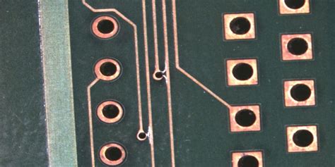
PTH is a method used in PCB Fabrication to create electrical connections between the different layers of a multi-layer PCB. It involves drilling holes through the board and then plating the inside of these holes with a conductive material, typically copper. This process ensures that electrical signals can pass through the board and reach their intended destinations, enabling the proper functioning of the electronic device.
The PCB Manufacturing Process and the Role of PTH
To understand the importance of PTH technology, it’s essential to have a basic understanding of the PCB manufacturing process. Here’s a simplified overview:
- Design: The PCB design is created using specialized software, defining the layout, components, and connections.
- Substrate Preparation: The base material, usually a fiberglass-reinforced epoxy laminate, is cut to the required size.
- Copper Cladding: Thin layers of copper foil are laminated onto both sides of the substrate.
- Drilling: Holes are drilled through the board at specific locations, as defined by the PCB design.
- Plating: The drilled holes are plated with copper to create electrical connections between layers (PTH).
- Patterning: The copper layers are patterned using a photolithography process to create the desired circuit traces.
- Etching: Unwanted copper is etched away, leaving only the desired circuit pattern.
- Solder Mask Application: A protective solder mask is applied to the board, exposing only the areas where components will be soldered.
- Surface Finish: A surface finish, such as HASL (Hot Air Solder Leveling) or ENIG (Electroless Nickel Immersion Gold), is applied to protect the exposed copper and enhance solderability.
- Silk Screen Printing: Text, symbols, and logos are printed onto the board for identification and assembly guidance.
- Quality Control: The manufactured PCBs undergo thorough inspections and tests to ensure quality and functionality.
PTH technology is employed in step 5 of this process, where the drilled holes are plated with copper. This step is crucial for several reasons:
- Electrical Connectivity: PTH ensures reliable electrical connections between the different layers of the PCB.
- Mechanical Strength: The plated holes provide mechanical support for through-hole components and help to anchor them securely to the board.
- Thermal Conductivity: PTH enhances the thermal conductivity of the board, allowing heat to dissipate more efficiently from components.

Advantages of PTH Technology
PTH technology offers several advantages in PCB manufacturing:
Reliable Electrical Connections
One of the primary benefits of PTH is the creation of reliable electrical connections between the different layers of a PCB. By plating the inside of the drilled holes with copper, PTH ensures that electrical signals can pass through the board without interruption. This is particularly important in multi-layer PCBs, where signals often need to traverse between layers to reach their intended destinations.
The copper plating process used in PTH creates a continuous, low-resistance path for electrical current. This helps to minimize signal loss and ensures that the electronic device functions as intended. The reliability of these connections is further enhanced by the fact that the copper plating adheres securely to the walls of the drilled holes, creating a robust mechanical and electrical bond.
Mechanical Strength and Durability
Another key advantage of PTH technology is the mechanical strength and durability it provides to the PCB. The plated holes not only create electrical connections but also serve as anchor points for through-hole components. When a component is inserted into a plated hole and soldered in place, it forms a strong mechanical bond with the board.
This mechanical anchoring is particularly important for components that are subject to physical stress or vibration. Without the support provided by the plated holes, these components could easily become loose or dislodged, leading to device failure. PTH ensures that components remain securely attached to the board, enhancing the overall durability and reliability of the electronic device.
Moreover, the plated holes themselves add to the structural integrity of the PCB. The copper plating reinforces the drilled holes, making them less susceptible to damage from handling or environmental factors. This added strength is especially beneficial in applications where the PCB may be exposed to harsh conditions or frequent use.
Thermal Management
PTH technology also plays a role in the thermal management of PCBs. Electronic components generate heat during operation, and this heat must be effectively dissipated to prevent damage and ensure optimal performance. The copper plating used in PTH helps to facilitate this heat dissipation.
Copper is an excellent thermal conductor, meaning it can efficiently transfer heat away from components and distribute it across the PCB. When a component is mounted in a plated hole, the copper plating provides a direct thermal path from the component to the board. This allows heat to be conducted away from the component more effectively, reducing the risk of overheating and improving overall thermal management.
In high-power applications or designs with high component density, PTH can be used in conjunction with thermal vias. Thermal vias are additional plated holes strategically placed near heat-generating components to further enhance heat dissipation. By providing more paths for heat to escape, thermal vias help to maintain acceptable operating temperatures and prevent thermal stress on components.

PTH vs. Surface Mount Technology (SMT)
While PTH technology offers several advantages, it’s important to note that it is not the only method used in PCB manufacturing. Surface Mount Technology (SMT) is another popular approach that has gained prominence in recent years. SMT involves mounting components directly onto the surface of the PCB, without the need for drilled holes.
Here’s a comparison of PTH and SMT:
| Aspect | PTH | SMT |
|---|---|---|
| Component Mounting | Through holes | Surface mount |
| Board Space | Requires more space due to drilled holes | Allows for higher component density |
| Component Size | Accommodates larger, through-hole components | Supports smaller, surface-mount components |
| Manufacturing Speed | Generally slower due to drilling and plating processes | Faster, as components are placed directly on the surface |
| Mechanical Strength | Provides strong mechanical anchoring for components | Relies on solder joints for mechanical strength |
| Thermal Management | Facilitates heat dissipation through plated holes | Limited thermal paths, may require additional thermal management techniques |
| Rework and Repair | Easier to replace or repair through-hole components | More challenging to rework or replace surface-mount components |
Despite the advantages of SMT, such as higher component density and faster manufacturing, PTH technology remains essential in PCB production. Many electronic designs still rely on through-hole components, particularly for power handling, high-current applications, or when mechanical strength is a priority. Additionally, some designs may require a combination of both PTH and SMT to achieve the desired functionality and performance.

Quality Control and Inspection Techniques for PTH
To ensure the reliability and integrity of PCBs manufactured with PTH technology, strict quality control and inspection procedures are necessary. Here are some common techniques used to assess the quality of plated through-holes:
Visual Inspection
Visual inspection is the first line of defense in quality control. Trained operators use magnification tools to visually examine the plated holes for any defects or anomalies. They look for issues such as incomplete plating, voids, cracks, or contamination. Visual inspection can help identify gross defects and provide a quick assessment of the overall quality of the PTH.
Microsectioning
Microsectioning involves cross-sectioning a sample PCB and examining the plated holes under a microscope. This destructive testing method allows for a detailed analysis of the plating thickness, uniformity, and adhesion to the hole walls. By measuring the plating thickness at different points along the hole, manufacturers can ensure that it meets the specified requirements and is consistent throughout the board.
Resistance Testing
Electrical resistance testing is used to verify the continuity and low resistance of the plated holes. This test involves measuring the resistance between the top and bottom surfaces of the board, as well as between different layers. A low resistance value indicates good electrical conductivity and a properly plated hole. High resistance or open circuits may suggest issues with the plating process or the presence of defects.
Thermal Stress Testing
Thermal stress testing exposes the PCB to extreme temperature variations to assess the reliability of the plated holes under thermal stress. The board is subjected to multiple cycles of high and low temperatures, simulating the conditions it may encounter during operation. This test helps identify any weaknesses in the plating or the bond between the plating and the hole walls, which could lead to failures in the field.
Solderability Testing
Solderability testing evaluates the ability of the plated holes to accept solder and form a reliable solder joint. A sample PCB is subjected to a controlled soldering process, and the resulting solder joints are inspected for quality and integrity. This test ensures that the plated holes are compatible with the soldering process and can provide a strong mechanical and electrical connection to the components.
By employing these quality control and inspection techniques, PCB Manufacturers can identify potential issues early in the production process and take corrective actions to maintain the highest standards of quality and reliability in their products.
Choosing the Right PCB Manufacturer for PTH
When it comes to PCB production, choosing the right manufacturer is crucial to ensure the quality and reliability of your electronic devices. Here are some key factors to consider when selecting a PCB manufacturer for projects involving PTH technology:
Experience and Expertise
Look for a manufacturer with a proven track record of producing high-quality PCBs using PTH technology. They should have experience in manufacturing boards similar to your specific requirements, such as multi-layer boards, high-density designs, or boards for harsh environments. Experienced manufacturers will have the knowledge and expertise to address any challenges that may arise during the production process.
Quality Management System
A reputable PCB manufacturer should have a robust quality management system in place. Look for certifications such as ISO 9001, which demonstrates their commitment to quality and continuous improvement. The manufacturer should follow stringent quality control procedures, including the inspection and testing techniques discussed earlier, to ensure the consistency and reliability of their products.
Manufacturing Capabilities
Consider the manufacturer’s technical capabilities and equipment. They should have state-of-the-art facilities and equipment capable of handling the specific requirements of your PTH project. This includes advanced drilling machines, plating equipment, and inspection tools. A manufacturer with a wide range of capabilities will be better equipped to meet your needs and provide flexibility in design and production.
Customer Support and Communication
Effective communication and responsive customer support are essential when working with a PCB manufacturer. Look for a manufacturer that is easy to communicate with and provides clear and timely responses to your inquiries. They should be willing to collaborate with you throughout the design and production process, offering guidance and support to ensure the best possible outcome for your project.
Lead Time and Pricing
Lead time and pricing are also important factors to consider. While it may be tempting to choose the lowest-cost option, keep in mind that quality should not be compromised. Look for a manufacturer that offers competitive pricing while maintaining high standards of quality. Additionally, consider their lead times and whether they can meet your production schedule without delays.
By carefully evaluating these factors and doing your due diligence, you can select a PCB manufacturer that will be a reliable partner for your PTH projects, ensuring the success and reliability of your electronic devices.
Frequently Asked Questions (FAQ)
1. What is the difference between PTH and non-plated through-holes?
PTH involves plating the inside of the drilled holes with a conductive material, typically copper, to create electrical connections between layers. Non-plated through-holes, also known as NPTHs, are simply drilled holes without any plating. NPTHs are used for mechanical purposes, such as mounting components or providing access for testing probes, but do not provide electrical connectivity between layers.
2. Can PTH be used with both through-hole and surface-mount components?
Yes, PTH technology is primarily used with through-hole components, which have leads that are inserted into the plated holes and soldered in place. However, PTH can also be used in conjunction with surface-mount components. In such cases, the plated holes serve as vias, providing electrical connections between layers, while the surface-mount components are placed on the surface of the board.
3. How does the aspect ratio of a plated hole affect the PCB design?
The aspect ratio of a plated hole refers to the ratio of the hole depth to its diameter. A higher aspect ratio (deeper hole relative to its diameter) can pose challenges in the plating process, as it becomes more difficult to ensure uniform plating throughout the entire depth of the hole. PCB designers need to consider the limitations of the manufacturing process and design the board accordingly, ensuring that the aspect ratios of plated holes are within acceptable ranges to maintain reliability and manufacturability.
4. What are the common defects associated with PTH, and how can they be prevented?
Common defects in PTH include incomplete plating, voids, cracks, and contamination. These defects can be caused by various factors, such as improper drilling, inadequate cleaning, or issues with the plating process. To prevent these defects, manufacturers must follow strict process controls, including proper hole preparation, thorough cleaning, and optimized plating parameters. Regular quality inspections and testing can help identify and address any issues early in the production process.
5. How does PTH technology impact the cost of PCB production?
PTH technology does add to the cost of PCB production compared to simple, single-layer boards without plated holes. The additional steps involved in drilling and plating the holes, as well as the increased complexity of multi-layer designs, contribute to higher manufacturing costs. However, the benefits of PTH, such as reliable electrical connections, mechanical strength, and thermal management, often justify the added cost in applications where performance and reliability are critical. The cost impact can be managed by optimizing the design, minimizing the number of layers and holes, and choosing a manufacturer with efficient processes and competitive pricing.
Conclusion
Plated through-hole technology is a critical component of modern PCB production. It enables reliable electrical connections between layers, provides mechanical strength and durability, and facilitates thermal management in electronic devices. While surface mount technology has gained prominence in recent years, PTH remains essential for many applications, particularly those involving through-hole components, high-power handling, or demanding mechanical requirements.
To ensure the quality and reliability of PCBs manufactured with PTH technology, manufacturers employ rigorous quality control and inspection techniques, including visual inspection, microsectioning, resistance testing, thermal stress testing, and solderability testing. These techniques help identify potential issues early in the production process and maintain the highest standards of quality.
When selecting a PCB manufacturer for projects involving PTH technology, it’s important to consider factors such as experience, expertise, quality management systems, manufacturing capabilities, customer support, lead time, and pricing. By carefully evaluating these factors, you can choose a manufacturer that will be a reliable partner in bringing your electronic devices to life.
As electronic devices continue to evolve and become more complex, the importance of PTH technology in PCB production will remain significant. By understanding the advantages, challenges, and best practices associated with PTH, designers and manufacturers can collaborate effectively to create high-quality, reliable electronic products that meet the ever-increasing demands of the market.


Leave a Reply