What is PCB Soldermask?
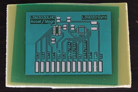
PCB soldermask, also known as solder resist or solder mask, is a thin layer of polymer that is applied to the copper traces of a printed circuit board (PCB). Its primary purpose is to protect the copper traces from oxidation, prevent solder bridges from forming between closely spaced pads, and provide electrical insulation.
Soldermask is typically applied using screen printing or photoimaging techniques. The most common colors for soldermask are green, red, blue, and black, although other colors are available for special applications.
Types of Soldermask
There are two main types of soldermask:
-
Liquid Photoimageable Soldermask (LPI): This type of soldermask is applied as a liquid and then exposed to UV light through a photomask to create the desired pattern. LPI soldermask is known for its high resolution and ability to cover fine details.
-
Dry Film Soldermask (DFS): DFS is a solid film that is laminated onto the PCB surface using heat and pressure. It is then exposed to UV light through a photomask and developed to create the desired pattern. DFS is known for its durability and resistance to harsh environments.
Common Problems with PCB Soldermask
Despite its importance in PCB manufacturing, soldermask can sometimes present various issues that affect the quality and reliability of the final product. Some of the most common problems include:
1. Pinholes and Voids
Pinholes and voids are small openings or gaps in the soldermask that expose the underlying copper. These defects can occur due to various reasons, such as:
- Improper cleaning of the PCB surface before applying soldermask
- Incorrect exposure or development time during the photoimaging process
- Contamination or air bubbles in the soldermask material
Pinholes and voids can lead to several issues, such as:
- Reduced insulation resistance between copper traces
- Increased risk of short circuits and solder bridges
- Corrosion of exposed copper due to environmental factors
Solutions for Pinholes and Voids
To minimize the occurrence of pinholes and voids, consider the following solutions:
-
Ensure proper cleaning of the PCB surface before applying soldermask. Use appropriate cleaning agents and techniques to remove any contaminants or residues.
-
Optimize the exposure and development parameters for the specific soldermask material and PCB design. Follow the manufacturer’s recommendations and conduct process control tests regularly.
-
Use high-quality soldermask materials from reputable suppliers. Ensure proper storage and handling of the soldermask to avoid contamination or degradation.
-
Implement strict quality control measures, such as visual inspection and electrical testing, to detect and reject PCBs with pinholes or voids.
2. Adhesion Issues
Adhesion issues occur when the soldermask does not properly adhere to the PCB surface or the copper traces. This can lead to delamination, peeling, or lifting of the soldermask, exposing the underlying copper to the environment.
Causes of adhesion issues include:
- Improper surface preparation or cleaning before applying soldermask
- Incompatibility between the soldermask and the PCB substrate material
- Insufficient curing or post-baking of the soldermask
- Mechanical stress or thermal shock during the manufacturing process or end-use application
Solutions for Adhesion Issues
To improve the adhesion of soldermask to the PCB surface, consider the following solutions:
-
Ensure proper surface preparation by cleaning the PCB thoroughly and roughening the surface if necessary to promote adhesion.
-
Select a soldermask material that is compatible with the PCB substrate and copper surface. Consult with the soldermask manufacturer or supplier for recommendations.
-
Follow the recommended curing and post-baking procedures for the specific soldermask material. Ensure that the temperature, time, and humidity parameters are within the specified ranges.
-
Design the PCB with adequate soldermask anchoring features, such as soldermask dams or anchoring holes, to provide mechanical support and prevent lifting or peeling.
3. Misregistration and Mismatch
Misregistration and mismatch occur when the soldermask pattern does not align properly with the copper pads or traces on the PCB. This can result in exposed copper or insufficient clearance between pads, leading to potential short circuits or soldering issues.
Causes of misregistration and mismatch include:
- Inaccurate alignment of the photomask or screen during the imaging process
- Dimensional changes in the PCB substrate due to thermal expansion or shrinkage
- Improper handling or transportation of the PCB during the manufacturing process
Solutions for Misregistration and Mismatch
To minimize misregistration and mismatch issues, consider the following solutions:
-
Use high-precision alignment equipment and techniques during the soldermask imaging process. Regularly calibrate and maintain the equipment to ensure accuracy and repeatability.
-
Compensate for the dimensional changes of the PCB substrate by adjusting the soldermask artwork or using special soldermask materials with low shrinkage properties.
-
Implement proper handling and transportation procedures to avoid physical distortion or damage to the PCB during the manufacturing process.
-
Incorporate fiducial marks or registration holes on the PCB and soldermask artwork to facilitate accurate alignment and registration.
4. Color Inconsistency and Fading
Color inconsistency and fading of the soldermask can occur due to various factors, such as:
- Improper mixing or inconsistent application of the soldermask material
- Exposure to UV light, high temperatures, or harsh chemicals during the manufacturing process or end-use application
- Degradation of the soldermask pigments or dyes over time
Color inconsistency and fading can affect the aesthetics of the PCB and make it difficult to identify components or markings.
Solutions for Color Inconsistency and Fading
To maintain consistent and durable soldermask color, consider the following solutions:
-
Use high-quality soldermask materials with stable pigments or dyes. Follow the manufacturer’s recommendations for mixing and application.
-
Control the exposure to UV light and high temperatures during the manufacturing process. Use UV filters or shielding materials if necessary.
-
Select soldermask materials with good chemical resistance properties for applications that involve exposure to harsh chemicals or solvents.
-
Implement color management systems and regular color testing to ensure consistency across different production batches and suppliers.
Frequently Asked Questions (FAQ)
1. What is the typical thickness of soldermask on a PCB?
The typical thickness of soldermask on a PCB ranges from 0.5 to 2 mils (12.7 to 50.8 microns). The exact thickness depends on the specific soldermask material, application method, and PCB design requirements.
2. Can soldermask be used on flexible PCBs?
Yes, soldermask can be used on flexible PCBs. However, special flexible soldermask materials are required to accommodate the bending and flexing of the PCB without cracking or delaminating. These materials typically have lower glass transition temperatures and higher elongation properties compared to standard soldermask materials.
3. How does soldermask affect the electrical properties of a PCB?
Soldermask acts as an insulating layer on the PCB surface, which can affect the electrical properties in several ways:
- It increases the surface insulation resistance (SIR) between adjacent copper traces, reducing the risk of leakage currents or short circuits.
- It can increase the capacitance between traces, especially if the soldermask has a high dielectric constant. This can affect the impedance and signal integrity of high-frequency circuits.
- It can also affect the thermal dissipation of the PCB, as the soldermask acts as a thermal barrier between the copper and the environment.
4. Can soldermask be removed or reworked if necessary?
Yes, soldermask can be removed or reworked if necessary, using mechanical or chemical methods. However, the process can be challenging and time-consuming, and it may damage the underlying copper or PCB substrate if not done carefully.
Mechanical methods involve scraping or sanding off the soldermask using abrasive tools or materials. Chemical methods involve using solvents or strippers to dissolve the soldermask material.
It is generally recommended to avoid removing or reworking soldermask unless absolutely necessary, as it can affect the reliability and performance of the PCB.
5. What are some alternative materials or technologies for PCB protection?
Some alternative materials or technologies for PCB protection include:
- Conformal coatings: These are thin, transparent coatings that are applied over the entire PCB surface, including the components and soldermask. They provide additional protection against moisture, dust, and chemical contamination.
- Potting compounds: These are thick, opaque materials that are used to encapsulate or embed the PCB and components in a solid block. They provide excellent mechanical and environmental protection but make the PCB difficult to repair or modify.
- Nanocoatings: These are ultra-thin, hydrophobic coatings that are applied using vapor deposition or plasma polymerization techniques. They provide a conformal, pinhole-free barrier against moisture and corrosion without significantly adding to the thickness or weight of the PCB.
- Bare PCBs: In some applications, such as high-frequency or microwave circuits, soldermask may be omitted altogether to minimize its impact on the electrical performance. The exposed copper is typically protected by a thin layer of organic solderability preservative (OSP) or immersion silver plating.

Conclusion
PCB soldermask is a critical component in the manufacturing of reliable and high-quality printed circuit boards. It provides essential protection against oxidation, solder bridging, and environmental factors while also improving the electrical insulation and aesthetics of the PCB.
However, soldermask is not without its challenges and potential issues. Common problems such as pinholes, adhesion loss, misregistration, and color inconsistency can affect the performance and reliability of the PCB if not addressed properly.
By understanding the causes and implementing appropriate solutions, PCB manufacturers and designers can minimize the occurrence of soldermask defects and ensure the long-term reliability of their products. This includes proper surface preparation, material selection, process control, and quality assurance measures.
As PCB technologies continue to evolve, so do the requirements and expectations for soldermask performance. Alternative materials and techniques, such as conformal coatings, nanocoatings, and bare PCBs, may be used in specific applications to overcome the limitations of traditional soldermask.
Ultimately, the choice of soldermask or alternative protection method depends on the specific requirements and constraints of the PCB application, such as the operating environment, electrical performance, manufacturability, and cost. By carefully considering these factors and working closely with material suppliers and process experts, PCB manufacturers can optimize their soldermask process and deliver high-quality, reliable products to their customers.

Leave a Reply