What is a Thru-hole Pad?
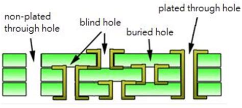
A thru-hole pad, also known as a plated through-hole (PTH), is a type of electrical connection used in printed circuit boards (PCBs). It consists of a hole drilled through the PCB, which is then plated with a conductive material, typically copper. This creates an electrical connection between the layers of the PCB and allows components to be soldered onto the board.
Thru-hole pads are used for mounting various electronic components, such as resistors, capacitors, and integrated circuits (ICs). They provide a robust mechanical and electrical connection, making them suitable for applications that require high reliability and durability.
Types of Thru-hole Pads
There are several types of thru-hole pads, each with its own characteristics and applications. The main types include:
1. Standard Thru-hole Pad
Standard thru-hole pads are the most common type used in PCB design. They have a circular shape and are typically plated with copper. The diameter of the hole and the size of the pad depend on the component being mounted.
2. Elongated Thru-hole Pad
Elongated thru-hole pads, also known as oval pads, have an elongated shape that allows for greater tolerance in component placement. They are useful when working with components that have leads with a larger diameter than the hole size.
3. Annular Ring Thru-hole Pad
Annular ring thru-hole pads have a circular pad with a concentric hole. The width of the annular ring (the distance between the hole and the outer edge of the pad) is an important factor in determining the strength of the solder joint.
4. Thermal Relief Thru-hole Pad
Thermal relief thru-hole pads are designed to reduce thermal stress during the soldering process. They have a spoke-like pattern of copper traces connecting the pad to the surrounding copper pour. This design allows heat to dissipate more evenly, preventing damage to the component or the PCB.

Thru-hole Pad Dimensions and Specifications
When designing a PCB with thru-hole pads, several dimensions and specifications must be considered to ensure proper functionality and manufacturability.
Hole Diameter
The hole diameter is the size of the drilled hole in the PCB. It is determined by the lead diameter of the component being mounted. The hole diameter should be slightly larger than the lead diameter to allow for easy insertion and proper soldering.
| Component Type | Typical Lead Diameter | Recommended Hole Diameter |
|---|---|---|
| Resistor | 0.5 mm | 0.8 mm |
| Capacitor | 0.5 mm | 0.8 mm |
| IC (DIP) | 0.5 mm | 0.8 mm |
| Connector | 1.0 mm | 1.2 mm |
Pad Diameter
The pad diameter is the size of the copper pad surrounding the hole. It should be large enough to provide a sufficient area for soldering and to ensure a strong mechanical connection.
| Hole Diameter | Minimum Pad Diameter | Recommended Pad Diameter |
|---|---|---|
| 0.8 mm | 1.6 mm | 2.0 mm |
| 1.0 mm | 1.8 mm | 2.2 mm |
| 1.2 mm | 2.0 mm | 2.4 mm |
Annular Ring Width
The annular ring width is the distance between the hole and the outer edge of the pad. A wider annular ring provides a stronger solder joint and better mechanical stability.
| Pad Diameter | Minimum Annular Ring Width | Recommended Annular Ring Width |
|---|---|---|
| 2.0 mm | 0.2 mm | 0.4 mm |
| 2.2 mm | 0.2 mm | 0.4 mm |
| 2.4 mm | 0.2 mm | 0.4 mm |
Copper Thickness
The copper thickness of the thru-hole pad affects its current-carrying capacity and the strength of the solder joint. Thicker copper layers provide better electrical and mechanical properties.
| Copper Weight | Copper Thickness |
|---|---|
| 1 oz/ft² | 35 µm |
| 2 oz/ft² | 70 µm |
| 3 oz/ft² | 105 µm |

Soldering Thru-Hole Pads
Soldering is the process of joining two metal surfaces by melting a filler metal (solder) between them. In the case of thru-hole pads, soldering is used to create a strong electrical and mechanical connection between the component leads and the PCB.
Soldering Methods
There are two main methods for soldering thru-hole pads:
-
Hand Soldering: This method involves using a soldering iron to manually apply solder to the pad and component lead. It is suitable for small-scale production or repairs.
-
Wave Soldering: This is an automated process where the PCB is passed over a molten solder wave, which coats the thru-hole pads and component leads. Wave soldering is used for large-scale production.
Solder Types
The type of solder used can affect the quality and reliability of the solder joint. The most common types of solder used for thru-hole pads are:
-
Lead-based Solder: Typically composed of 63% tin and 37% lead (Sn63/Pb37), this solder has a low melting point and good wetting properties. However, due to environmental and health concerns, its use is being phased out.
-
Lead-free Solder: These solders are composed of various alloys, such as tin-silver-copper (SAC) or tin-copper (SnCu). They have higher melting points and require more precise temperature control during soldering.
Soldering Quality
The quality of the solder joint is critical for the reliability and functionality of the PCB. A good solder joint should have the following characteristics:
- Complete filling of the thru-hole pad with solder
- A concave fillet around the component lead and pad
- Shiny and smooth surface
- No voids, cracks, or excess solder
Common soldering defects include:
- Insufficient solder: The solder does not fill the hole completely, resulting in a weak connection.
- Excess solder: Too much solder is applied, which can cause short circuits or bridging between adjacent pads.
- Cold joint: The solder does not melt properly, resulting in a dull, grainy appearance and poor electrical connection.
- Solder bridge: Excess solder creates an unintended connection between two or more pads.

Thru-hole Pad Inspection and Testing
After soldering, it is essential to inspect and test the thru-hole pads to ensure the quality and reliability of the solder joints.
Visual Inspection
Visual inspection is the first step in assessing the quality of the solder joints. This can be done using a magnifying lens or microscope. Inspectors look for the following:
- Complete hole fill
- Proper fillet formation
- Absence of defects (e.g., voids, cracks, bridges)
Automated Optical Inspection (AOI)
AOI uses cameras and image processing software to automatically inspect solder joints. It can detect defects such as insufficient solder, excess solder, and solder bridges. AOI is particularly useful for high-volume production, as it can quickly inspect a large number of solder joints.
X-ray Inspection
X-ray inspection is used to detect defects that are not visible from the surface, such as voids or cracks within the solder joint. This method is particularly useful for inspecting solder joints under components with high lead counts, such as ball grid array (BGA) packages.
Electrical Testing
Electrical testing is used to verify the continuity and insulation resistance of the solder joints. This can be done using a multimeter or a dedicated continuity tester. Electrical testing ensures that the solder joints are functioning as intended and that there are no short circuits or open connections.
FAQ
1. What is the difference between a thru-hole pad and a surface mount pad?
A thru-hole pad has a hole drilled through the PCB, and the component lead is inserted through the hole and soldered on the opposite side. A surface mount pad, on the other hand, is a flat copper area on the surface of the PCB, and the component is soldered directly onto the pad without a hole.
2. Can thru-hole pads be used for surface mount components?
Yes, thru-hole pads can be used for surface mount components by using a technique called “dead-bug” mounting. In this method, the surface mount component is glued upside-down onto the PCB, and its leads are bent and soldered to the thru-hole pads.
3. What is the advantage of using thermal relief thru-hole pads?
Thermal relief thru-hole pads help to dissipate heat more evenly during the soldering process, reducing thermal stress on the component and the PCB. This helps to prevent damage and improves the reliability of the solder joint.
4. How do I choose the right solder for my thru-hole pads?
The choice of solder depends on several factors, including the type of components being used, the soldering method, and environmental considerations. Lead-free solders are becoming more common due to environmental and health concerns, but they require more precise temperature control during soldering. It is essential to consult the component manufacturer’s recommendations and follow industry standards when selecting a solder.
5. What should I do if I detect a defect in a thru-hole pad solder joint?
If a defect is detected in a thru-hole pad solder joint, the appropriate action depends on the type and severity of the defect. Minor defects, such as insufficient solder, can often be repaired by adding more solder. More severe defects, such as voids or cracks, may require the joint to be desoldered and resoldered. In some cases, the component may need to be replaced entirely. It is essential to follow proper repair procedures and to re-inspect the joint after the repair to ensure its quality and reliability.
Conclusion
Thru-hole pads are an essential component of PCB design, providing a robust mechanical and electrical connection for electronic components. Understanding the different types of thru-hole pads, their dimensions and specifications, and the soldering process is crucial for designing and manufacturing high-quality, reliable PCBs.
Proper inspection and testing of thru-hole pad solder joints are also critical for ensuring the functionality and longevity of the PCB. By following industry standards and best practices, PCB designers and manufacturers can create thru-hole pad connections that meet the demanding requirements of modern electronic devices.
As technology continues to evolve, the use of thru-hole pads may decline in favor of surface mount techniques, which offer smaller footprints and higher component densities. However, thru-hole pads will likely remain an important part of PCB design for applications that require high reliability, durability, and power handling capabilities.
By staying up-to-date with the latest developments in thru-hole pad technology and soldering techniques, PCB designers and manufacturers can continue to create innovative, high-quality electronic devices that meet the needs of a wide range of industries and applications.


Leave a Reply