Surface mount technology (SMT) is a method of assembling printed circuit boards (PCBs) where the electronic components are mounted directly onto the surface of the board rather than through holes. This allows for smaller and more compact PCB designs compared to through-hole assembly. There are several benefits to using SMT:
- Smaller components – Surface mount components are much smaller than their through-hole counterparts. This allows for tighter spacing and more compact board designs.
- Higher component density – With smaller components and tighter spacing, many more components can be fit onto a single PCB. This is especially useful for complex and compact devices.
- Automated assembly – SMT lends itself well to automated assembly with pick-and-place machines, making the process faster and more efficient at scale.
- Improved performance – The smaller size of SMT components enables shorter traces and connections, giving better high-frequency performance.
- Double-sided mounting – Both sides of the board can be utilized for component placement.
- Cost – Despite higher upfront costs for SMT equipment, reduced labor and material costs make it cheaper at scale.
Some common types of surface mount components include integrated circuits (ICs), resistors, capacitors, transistors, and LEDs. The components have leads or terminals designed for surface mounting and are typically supplied in tape-and-reel packaging for use in automated assembly.
SMT Assembly Process Overview

Here is a general overview of the surface mount PCB assembly process:
1. PCB Design
The PCB must be designed specifically for surface mount components with the appropriate land patterns and clearances. CAD software is used to design the board layout and routing.
2. Stencil Creation
A metal stencil is created with cutouts matching the land patterns of the SMT components for the solder paste application. Stencils are typically made from stainless steel or nickel-plated brass sheets.
3. Solder Paste Application
Solder paste containing powdered solder alloy and flux is applied onto the PCB through the stencil openings using a squeegee. This deposits precise amounts of solder paste where components will be placed.
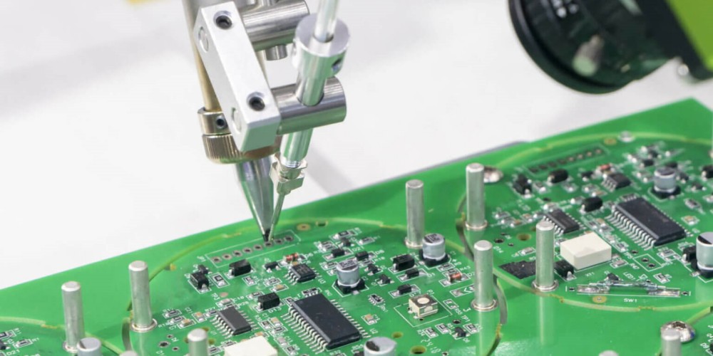
4. Component Placement
SMT components are precisely placed in their designated locations on the board either manually or using automated pick-and-place machines. High-speed machines can place over 25,000 components per hour.
5. Reflow Soldering
The board passes through a reflow oven with a carefully controlled thermal profile, melting the solder paste to form reliable solder joints and attaching the components. Different profiles are used for lead-free or leaded solder.
6. Inspection and Testing
PCBs are visually inspected for defects, then electrically tested to verify the board and components function properly according to specifications. Automated optical inspection (AOI) systems are often used.
7. Conformal Coating
A protective polymer coating may be applied to provide environmental and insulation protection for the assembled board and components.
8. Quality Assurance
Statistical quality control is performed and continuous improvement tracked throughout the process to meet quality standards and requirements.
SMT Equipment
Specialized equipment is required to assemble SMT boards efficiently and reliably:
Solder Paste Printers
Apply precise amounts of solder paste to board through stencil. Features like automatic stencil cleaning help maintain accuracy.
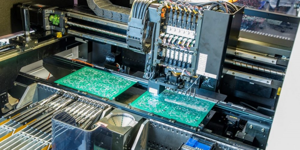
Pick-and-Place Machines
Automatically pick components from tapes/trays and place in position on PCB.High accuracy and speed with multiple heads and feeders.
Reflow Ovens
Use thermal profile with infrared heating and forced air convection to solder components. Different zones control preheat, reflow, and cooling.
AOI Systems
Automated optical inspection checks for defects and accuracy after soldering using high-resolution cameras. Can detect faults down to 0.025mm.
Conformal Coating Systems
Dispense and cure protective polymer coatings onto assembled PCBs for insulation and environmental resistance. Can be spray or vapor deposition.
X-Ray Inspection
X-ray imaging is used to check for hidden solder joint defects and verify proper assembly without destructive testing.
Test Equipment
Testing equipment like flying probe testers electrically verify assembled boards meet electronic specifications and quality standards.
Proper setup, calibration, and maintenance of SMT equipment is crucial for optimizing production quality and yields. Working closely with equipment vendors is recommended.
SMT Design Considerations
The PCB design can greatly impact the efficiency and success of SMT assembly. Here are some key considerations:
- Component spacing – Adequate spacing between components for pick-and-place clearance and solder paste application.
- Land pattern geometry – Match land patterns to component leads for sufficient solder joint fillet size.
- Solder mask defined vs non solder mask defined pads – Determines how solder paste is constrained on pads.
- High-density component placement – Group components intelligently to optimize pick-and-place machine efficiency.
- Avoid tombstoning – Use symmetrical land patterns to prevent tilted components during reflow.
- Thermal relief connections – Prevent solder cracking for high thermal expansion components.
- Component orientation – Consistent orientation of polarized components like diodes and ICs.
- Fine-pitch parts – Requires tighter tolerances – below 0.5mm component pitch requires advanced processes.
- Double-sided assembly – Requires concurrent reflow of top and bottom sides.
Following SMT design guidelines from the IPC association is highly recommended for robust and manufacturable PCB designs.
SMT Assembly Challenges
While SMT provides many benefits, some common challenges can impact quality and yield:
Solder Paste Printing Issues
- Clogged stencil apertures due to dried paste can cause insufficient print deposits.
- Paste slumping if the stencil separates from the PCB can lead to solder bridges.
- Insufficient stencil cleaning regimes can reduce print quality over time.
Pick-and-Place Errors
- Tombstoning where components stand vertically due to uneven paste deposits or polarity issues.
- Shifted components if the pick-and-place accuracy is insufficient.
- Misloaded components or incorrect orientations.
- Damaged components due to impact forces.
Reflow Defects
- Incomplete solder joint formation if paste volumes are insufficient.
- Excessive solder bead height if too much paste is deposited.
- Solder balling due to excessive paste or non-wetting surfaces.
- Solder bridging if paste volumes are too high or clearances are inadequate.
- Thermal shock cracking of components from high thermal gradients.
Other Defects
- Mechanical damage of boards or components during handling.
- Electromagnetic interference causing issues for sensitive components.
- Contamination from dirt, debris, or chemicals.
- Electrostatic discharge (ESD) damaging components.
Implementing robust process controls, inspection methods, operator training, and continuous improvement is key to minimizing defects and maximizing SMT quality and yields.
Advantages of Outsourcing SMT Assembly
Many companies outsource SMT production to contract electronics manufacturers (CEMs/EMS providers) to leverage benefits like:
- Expertise and capabilities – Access specialized equipment, expertise, and well-established processes.
- Scalability – Ability to scale up or down production volumes as needed. Avoid costs of in-house equipment.
- Supply chain – Assistance with complex global supply chains and component sourcing.
- Quality – Consistent quality standards and product reliability.
- Cost efficiency – Lower labor costs and economies of scale achieve optimal cost efficiency.
- Low volumes – Contract manufacturers specialize in supporting low to high volumes cost effectively.
- Turnkey services – From prototype builds through full production – PCB assembly, testing, enclosure fabrication, etc.
- Focus on core competencies – In-house teams can focus on design and engineering rather than manufacturing.
However, loss of control over intellectual property and lead times extending beyond internal targets are risks to weigh. Carefully qualifying and selecting the right contract manufacturer is key to success.
Conclusion
Surface mount assembly enables smaller, faster, and lower cost PCB manufacturing compared to through-hole techniques. But realizing these benefits requires careful process engineering and attention to detail. Working with an experienced SMT assembly partner combines expertise with flexible capacity to meet modern electronic production needs.
Frequently Asked Questions
What are some key steps in the SMT assembly process?
Some of the major steps are: solder paste printing, component placement, reflow soldering, inspection/testing, and quality assurance. Proper PCB design, stencil fabrication, solder paste application, and reflow profile are critical sub-processes.
What types of defects can occur in SMT assembly?
Common SMT defects include tombstoning, solder bridges, insufficient solder joints, thermal cracks, paste printing issues, component shifts, ESD damage, contamination, and more. Robust process control and inspection regimes help minimize defects.
What design considerations help enable reliable SMT assembly?
Adequate component spacing, thermal relief connections, avoiding tombstoning, sufficient land sizes, proper pad geometries, consistent component orientations, and following IPC guidelines help create SMT-friendly PCB designs.
How does outsourced manufacturing help with SMT production?
Outsourcing provides access to expertise, specialized equipment, scalability, supply chain assistance, and improved cost efficiency. It allows focusing internal resources on core design strengths.
What risks come with outsourcing SMT assembly?
Potential downsides of outsourcing include loss of direct control over IP and processes, as well as lead times extending beyond internal targets if not managed proactively. Carefully selecting the right partner minimizes these risks.


Leave a Reply