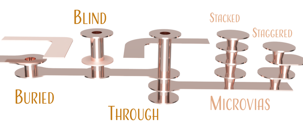
Microvias are small vias used to connect different layers in a multilayer printed circuit board (PCB). Staggering these microvias instead of stacking them directly on top of each other provides several advantages in PCB design. This article explores what staggered microvias are, why they are used, and their key benefits.
What Are Staggered Microvias?
A microvia is a small via typically ranging from 0.1 mm to 0.25 mm in diameter used to interconnect two or more adjacent layers in a PCB. Microvias enable routing connections between layers that would otherwise be difficult or impossible with standard-sized vias.
However, when multiple microvias are placed directly on top of each other to span more than two layers, issues can arise during the manufacturing process. The main problem is that it is difficult to achieve reliable plating of the barrels of stacked microvias during electroless copper plating.
To avoid these plating issues, microvias can be staggered or offset from each other. Staggered microvias follow a pattern of being placed side-by-side rather than directly stacked. This allows for more reliable plating while still providing interlayer connections across several layers.
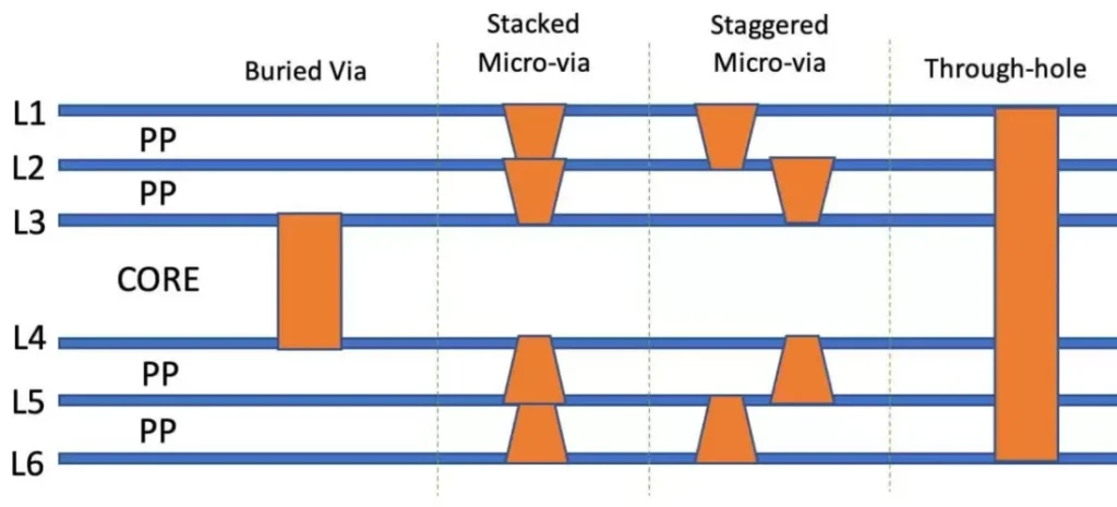
Here is a diagram comparing stacked and staggered microvia configurations:<table> <tr> <th>Stacked Microvias</th> <th>Staggered Microvias</th> </tr> <tr> <td>
Show Image</td> <td>
Show Image</td> </tr> </table>
As you can see, the staggered microvias form a stepping stone pattern between layers rather than a straight vertical stack.
Why Use Staggered Microvias?
There are several key benefits to using staggered microvias instead of stacking them vertically:
1. Improved Plating Reliability
As mentioned previously, the main advantage of staggered microvias is more reliable plating, especially during electroless copper plating. With a stacked configuration, the plating solution has difficulty reaching and depositing copper deep within the vertical via barrel. Staggering creates a less constrained path that improves solution access and plating consistency.
2. Reduced Drilling Issues
Drilling stacked microvias requires precise laser beam alignment to hit the small target area on each layer. Even tiny drilling inaccuracies can result in misalignments. Staggering relaxes the positioning tolerance requirements and allows for more margin of error when drilling across layers.
3. Lower Aspect Ratio
The aspect ratio is the ratio of the microvia barrel height to its diameter. High aspect ratio microvias with a tall, narrow shape can create plating problems. Staggering microvias lowers the aspect ratio on each individual via, making them easier to plate reliably.
4. Optimized Routing
Staggered microvias often allow for more optimized routing than stacked vias. The stepping stone pattern can navigate around components and traces more easily, avoiding congestion. This facilitates routing dense PCB designs.
5. Reduced Stresses
Thermal stresses can develop around plated through-holes in PCBs. Stacking microvias concentrates this stress while staggering helps dissipate it by spreading vias across the board. This improves reliability and reduces risk of cracks or failures.
6. Design Flexibility
Staggered microvias give designers more flexibility when laying out the board. Vias can be placed in locations that avoid interfering with routing or components. This flexibility is limited with stacked vias since they must be precisely aligned.
Implementing Staggered Microvias in PCBs
Layer Planning
The first step is planning which layers the microvias will interconnect. This includes choosing the total number of layers and determining if microvias are needed between each adjacent layer or if skipping layers is acceptable.
Depth Matching
Microvias between two layers should be drilled to match the total depth between layers. For example, a 4-layer board may have:
- Layer 1 to Layer 2: 50μm depth
- Layer 2 to Layer 3: 150μm depth
The microvias between Layers 1 and 2 are drilled to 50μm while those between Layers 2 and 3 are 150μm.
Laser Drilling
A laser is typically used to accurately drill the microvias. Laser drilling machines can be programmed with the precise locations and depths of each staggered microvia.
Layout Rules
It helps to establish layout rules for the minimum/maximum distance between microvias and from their edges to pads, traces, etc. This ensures reliable fabrication and assembly.
Interlayer Connections
Microvia pads are added on each layer to connect traces entering/exiting the via. Thermal reliefs can help reduce stresses.
Filling and Plating
The drilled microvias are plated with electroless copper then filled with epoxy or similar dielectric material. Additional copper plating can provide capping.
Via Protection
Solder mask tenting over microvias helps protect from environmental contamination. Plugging microvias after soldering is another protection option.
Staggered Microvia Patterns
There are several common patterns used when placing staggered microvias:
Stepping Stone
Each via steps across in an X-Y diagonal grid pattern from one layer to the next. This provides optimal plating access and routing flexibility.
Perimeter Stagger
Vias are clustered near the component or routing channel perimeter and staggered diagonally outward. Helps concentrate interlayer connections.
Double Stagger
Vias are staggered first in one diagonal direction then the other direction on the next layer. Forms a denser microvia field.
Corss Stagger
Vias are staggered horizontally on one layer then vertically on the next layer. Can provide symmetry and uniform spacing.
Multi-Direction Stagger
Vias are staggered across each layer with no fixed pattern. Provides the most flexibility but can be tricky to fabricate.
Staggered Microvia FAQ
Here are answers to some frequently asked questions about staggered microvias:
How are staggered microvias fabricated?
They are fabricated using a sequence of laser drilling, metallization, filling, and plating steps. Each microvia is laser drilled to the planned depth at precise x-y locations. The vias are then plated with electroless copper, filled with epoxy, capped with more plating, and optionally tented with solder mask.
Do microvias require special PCB stackups?
Yes, the layer stackup must be designed specifically to accommodate interlayer microvias at the planned depths. The dielectric materials used in the multilayer construction must also be compatible with laser drilling.
Can microvias go through flex PCBs?
Yes, but spacing, density, and layout requires special consideration to avoid cracking in flexible PCBs. Staggering helps by lowering stresses. Slotted pads also help relieve stresses around flex microvias.
What are the minimum and maximum sizes for microvias?
The typical range is 0.1mm to 0.25mm in diameter. Aspect ratios up to 1:1 are common. Ultra-high-density designs may use sub-0.1mm microvias. The smallest mechanically drilled production vias are around 0.15mm presently.
How do I design routes between staggered microvia layers?
It helps to visualize routing channels between the “stepping stones” created by the staggered vias. The vias can jog the routing layers to transition between the channels. Solid planes may need split into regions between channels.
Can microvias go through or under BGAs?
It is best to avoid placing microvias under the BGA footprint since drilling debris can interfere with solder joint reliability. Staggering or slotting vias at the BGA perimeter is recommended instead.
Conclusion
Implementing staggered microvias offers significant advantages compared to stacking microvias vertically in multilayer PCBs. The ability to reliably plate staggered configurations allows for high-density interconnections spanning several layers. Careful planning is required to best leverage the benefits of staggered microvias and avoid potential pitfalls. As PCBs become more complex, staggered microvias present an enabling technology to achieve routing and circuit density goals.


Leave a Reply