Introduction to Solder Paste Printing
Solder paste printing is a crucial step in the surface mount technology (SMT) assembly process. It involves depositing solder paste onto the pads of a printed circuit board (PCB) using a stencil. The accuracy and consistency of solder paste printing directly impact the quality and reliability of the final assembled product. In this article, we will discuss some valuable tips for optimizing your solder paste printing process.
Importance of Solder Paste Printing
Solder paste printing is the foundation of a successful SMT assembly. It is responsible for providing the right amount of solder paste at the correct locations on the PCB. If the solder paste is not printed accurately, it can lead to a variety of defects such as:
- Insufficient solder joints
- Bridging between adjacent pads
- Tombstoning of components
- Solder balls and splashes
These defects can cause reliability issues and even complete failure of the assembled product. Therefore, it is essential to optimize the solder paste printing process to minimize these defects and ensure high-quality assemblies.

Factors Affecting Solder Paste Printing
Several factors can affect the quality of solder paste printing. These include:
- Stencil design and quality
- Solder paste properties
- Printer settings and maintenance
- PCB design and quality
- Environmental conditions
Let’s discuss each of these factors in more detail.
Stencil Design and Quality
The stencil is the most critical component of the solder paste printing process. It determines the amount and placement of solder paste on the PCB. Here are some tips for stencil design and quality:
- Use a stencil thickness that matches the solder paste particle size and PCB pad size. A typical stencil thickness is 0.1 mm to 0.15 mm.
- Ensure that the stencil apertures are correctly sized and shaped for each pad. The aperture should be slightly larger than the pad to allow for solder paste release.
- Use a stencil material that is compatible with your solder paste and cleaning process. Stainless steel is the most common material, but nickel-plated and laser-cut stencils are also available.
- Regularly inspect the stencil for damage, wear, and contamination. Clean or replace the stencil as needed.
Solder Paste Properties
The solder paste itself also plays a crucial role in the printing process. Here are some tips for selecting and handling solder paste:
- Choose a solder paste that is compatible with your stencil, PCB, and components. Consider factors such as alloy composition, particle size, and flux activity.
- Store the solder paste at the recommended temperature and humidity levels to maintain its rheological properties.
- Regularly check the solder paste for signs of degradation, such as separation of the flux and metal particles or changes in viscosity.
- Use a solder paste with a consistent print volume and release characteristics to ensure repeatable results.
Printer Settings and Maintenance
The solder paste printer is another critical component of the printing process. Here are some tips for setting up and maintaining your printer:
- Calibrate the printer regularly to ensure accurate positioning and pressure settings.
- Use a print speed and pressure that are appropriate for your solder paste and PCB design. A typical print speed is 20 mm/s to 50 mm/s, and a typical pressure is 0.2 kg to 0.5 kg.
- Maintain a consistent print gap between the stencil and PCB. A typical gap is 0.5 mm to 1 mm.
- Clean the printer, stencil, and squeegee regularly to prevent contamination and ensure consistent print quality.
PCB Design and Quality
The design and quality of the PCB itself can also affect the solder paste printing process. Here are some tips for PCB design and quality:
- Ensure that the PCB pads are correctly sized and spaced for the components and stencil apertures.
- Use a soldermask that is compatible with your solder paste and has good adhesion to the PCB.
- Ensure that the PCB surface is clean, flat, and free of debris or contamination.
- Use a PCB material that is compatible with your reflow process and has good thermal stability.
Environmental Conditions
Finally, environmental conditions such as temperature and humidity can also affect the solder paste printing process. Here are some tips for controlling environmental conditions:
- Maintain a consistent room temperature of 20°C to 25°C and a relative humidity of 30% to 60%.
- Avoid drafts or air currents that can cause the solder paste to dry out or shift on the PCB.
- Use a controlled storage environment for the solder paste and PCBs to prevent moisture absorption or oxidation.

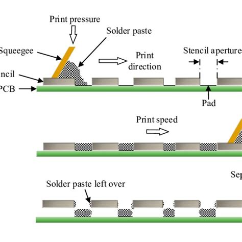
Solder Paste Printing Process
Now that we’ve discussed the factors affecting solder paste printing, let’s go through the printing process step by step.
Step 1: Stencil Alignment
The first step is to align the stencil with the PCB. This is typically done using fiducial marks on the stencil and PCB. The printer uses a vision system to locate the fiducial marks and adjust the position of the stencil accordingly.
Step 2: Solder Paste Application
Next, the solder paste is applied to the stencil using a squeegee. The squeegee moves across the stencil, forcing the solder paste through the apertures and onto the PCB pads. The squeegee pressure and speed are critical parameters that affect the amount and consistency of the solder paste deposit.
Step 3: Stencil Release
After the solder paste is applied, the stencil is released from the PCB. This is typically done by lifting the stencil vertically away from the PCB. The speed and angle of the stencil release can affect the shape and volume of the solder paste deposit.
Step 4: Inspection
After the stencil is released, the PCB is inspected to ensure that the solder paste has been correctly deposited on the pads. This is typically done using a solder paste inspection (SPI) system that uses 2D or 3D imaging to measure the volume, height, and shape of the solder paste deposits.
Step 5: Cleaning
Finally, the stencil is cleaned to remove any residual solder paste and prevent contamination of future prints. This is typically done using a stencil cleaning machine that uses a solvent or ultrasonic cleaning process.

Troubleshooting Common Solder Paste Printing Defects
Despite our best efforts, solder paste printing defects can still occur. Here are some common defects and their possible causes and solutions:
| Defect | Possible Causes | Solutions |
|---|---|---|
| Insufficient solder paste | – Stencil apertures too small – Solder paste too thick – Squeegee pressure too low |
– Increase aperture size – Reduce solder paste viscosity – Increase squeegee pressure |
| Bridging between pads | – Stencil apertures too close together – Solder paste too thin – Squeegee speed too high |
– Increase aperture spacing – Increase solder paste viscosity – Reduce squeegee speed |
| Solder balls and splashes | – Stencil release too slow – Solder paste too thin – PCB surface contaminated |
– Increase stencil release speed – Increase solder paste viscosity – Clean PCB surface |
| Stencil clogging | – Solder paste too thick – Stencil apertures too small – Insufficient stencil cleaning |
– Reduce solder paste viscosity – Increase aperture size – Improve stencil cleaning process |
Best Practices for Solder Paste Printing
To optimize your solder paste printing process and minimize defects, follow these best practices:
- Use a high-quality stencil with the correct aperture size and shape for your PCB and components.
- Select a solder paste that is compatible with your stencil, PCB, and reflow process, and has consistent print volume and release characteristics.
- Calibrate and maintain your solder paste printer regularly, including the squeegee, stencil, and vision system.
- Design your PCB with appropriate pad sizes and spacing for the stencil apertures and components.
- Control environmental conditions such as temperature and humidity to prevent solder paste degradation or contamin
ation.
– Inspect the solder paste deposits after printing using an SPI system to ensure correct volume, height, and shape.
– Clean the stencil regularly using a stencil cleaning machine or manual cleaning process.
FAQ
1. What is the recommended stencil thickness for solder paste printing?
A typical stencil thickness is 0.1 mm to 0.15 mm, depending on the solder paste particle size and PCB pad size. Thicker stencils may be needed for larger pads or higher-viscosity solder pastes.
2. How often should I clean my solder paste printer?
The frequency of cleaning depends on the usage and environment of the printer. In general, it is recommended to clean the stencil after every shift or every 1,000 prints, whichever comes first. The squeegee and other parts of the printer should be cleaned on a regular basis according to the manufacturer’s recommendations.
3. Can I use the same solder paste for different PCB designs?
It is possible to use the same solder paste for different PCB designs, but it is important to ensure that the solder paste is compatible with the stencil apertures, pad sizes, and reflow profile of each design. It may be necessary to adjust the printer settings or stencil design to optimize the solder paste deposit for each PCB.
4. What is the shelf life of solder paste?
The shelf life of solder paste depends on the specific product and storage conditions. Most solder pastes have a shelf life of 6 to 12 months when stored at the recommended temperature and humidity levels. It is important to check the expiration date and storage requirements of the solder paste before use.
5. How can I prevent solder paste from drying out during the printing process?
To prevent solder paste from drying out, it is important to control the environmental conditions of the printing area, such as temperature and humidity. The solder paste should be stored in a sealed container when not in use, and the stencil should be cleaned regularly to prevent contamination. Some printers also have a built-in humidity control system to maintain the optimal conditions for solder paste.
Conclusion
Solder paste printing is a critical step in the SMT assembly process that requires careful optimization to ensure high-quality and reliable results. By following the tips and best practices outlined in this article, you can improve the accuracy, consistency, and repeatability of your solder paste printing process. Remember to select the right stencil, solder paste, and printer settings for your specific PCB design and components, and to regularly inspect and maintain your equipment to prevent defects and ensure long-term success.


Leave a Reply