Introduction to Via-hole soldermask
Via-holes are an essential component in printed circuit board (PCB) design, providing electrical connections between different layers of a multilayer board. The application of soldermask on via-holes is a crucial process that ensures the reliability and functionality of the PCB, especially when using a chemical Nickel-Gold (ENIG) surface finish. This article will explore the importance of via-hole soldermask, its application process, and the benefits it offers in the context of ENIG surface finish.
What is a via-hole?
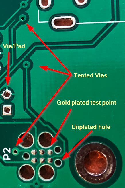
A via-hole, or simply a via, is a small hole drilled through a PCB to create an electrical connection between different layers of the board. Vias can be classified into three main types:
- Through-Hole Vias: These vias extend through the entire thickness of the PCB, connecting all layers.
- Blind Vias: These vias start from one surface of the PCB and terminate at an inner layer, without reaching the opposite surface.
- Buried Vias: These vias are located entirely within the inner layers of the PCB, without extending to either surface.
The role of soldermask in PCB manufacturing
Soldermask, also known as solder resist or solder stop, is a thin layer of polymer applied to the surface of a PCB. Its primary functions include:
- Protecting the copper traces from oxidation and corrosion
- Preventing solder bridges between closely spaced pads or traces
- Providing electrical insulation between conductive areas
- Improving the aesthetics of the PCB by providing a uniform color (typically green)
The importance of via-hole soldermask in ENIG surface finish
Understanding ENIG surface finish
ENIG (Electroless Nickel Immersion Gold) is a popular surface finish for PCBs due to its excellent solderability, flat surface, and long shelf life. The ENIG process involves the following steps:
- Cleaning the copper surface
- Applying a thin layer of electroless nickel (typically 3-6 µm)
- Applying a thin layer of immersion gold (typically 0.05-0.2 µm) over the nickel layer
The nickel layer serves as a barrier to prevent copper migration, while the gold layer provides protection against oxidation and enhances solderability.
Challenges in applying soldermask on via-holes with ENIG finish
Applying soldermask on via-holes in PCBs with ENIG surface finish can be challenging due to several factors:
- Inconsistent soldermask coverage: The small size and high aspect ratio of via-holes can make it difficult to achieve consistent soldermask coverage, leading to exposed copper or thin soldermask layers.
- Compatibility issues: Some soldermask materials may not adhere well to the ENIG surface, resulting in poor adhesion or delamination.
- Soldermask plug formation: Excess soldermask material can accumulate inside the via-holes, forming soldermask plugs that can hinder the ENIG process and affect the electrical connection.
Benefits of proper via-hole soldermask application
When applied correctly, via-hole soldermask offers several benefits in PCBs with ENIG surface finish:
- Enhanced reliability: Proper soldermask coverage protects the via-holes from contamination and corrosion, improving the overall reliability of the PCB.
- Improved ENIG performance: By preventing excess soldermask from accumulating inside the via-holes, the ENIG process can be carried out more effectively, resulting in better nickel and gold coverage.
- Reduced risk of solder defects: Soldermask helps prevent solder from wicking into the via-holes during the assembly process, reducing the risk of solder defects such as solder bridges or insufficient solder joints.
Via-hole soldermask application process
Pre-treatment of via-holes
Before applying soldermask, via-holes must be properly cleaned and prepared to ensure good adhesion and coverage. The pre-treatment process typically involves the following steps:
- Desmear: This process removes the resin smear from the via-hole walls, which is caused by the drilling process. Desmearing can be done chemically (using permanganate or plasma) or mechanically (using abrasive materials).
- Electroless copper plating: A thin layer of electroless copper (typically 0.5-1 µm) is deposited onto the via-hole walls to improve the adhesion of the subsequent soldermask layer.
- Cleaning: The PCB is thoroughly cleaned to remove any contaminants or residues that may affect soldermask adhesion.
Soldermask application methods
There are several methods for applying soldermask on via-holes, each with its advantages and limitations:
- Screen printing: This is the most common method for applying soldermask. A stencil with the desired soldermask pattern is placed over the PCB, and the soldermask material is forced through the openings using a squeegee. Screen printing offers good thickness control and is suitable for high-volume production.
- Spray coating: In this method, soldermask is sprayed onto the PCB surface using a spray gun. Spray coating is suitable for low-volume production and can achieve a more uniform coverage compared to screen printing.
- Liquid photoimageable (LPI) soldermask: LPI soldermask is applied as a liquid and then exposed to UV light through a photomask to selectively cure the desired areas. LPI soldermask offers high resolution and is suitable for fine-pitch designs.
- Inkjet printing: This is an emerging technology that uses inkjet printers to deposit soldermask material onto the PCB surface. Inkjet printing offers high precision and can be used for small-batch production or prototyping.
Soldermask curing
After application, the soldermask must be cured to achieve its final properties. Curing is typically done using one of the following methods:
- Thermal curing: The PCB is heated to a specific temperature (usually 150-180°C) for a certain duration (30-90 minutes) to crosslink the soldermask polymer.
- UV curing: The soldermask is exposed to UV light to initiate the crosslinking reaction. UV curing is faster than thermal curing but requires a UV-sensitive soldermask formulation.

Factors affecting via-hole soldermask performance
Several factors can influence the performance of via-hole soldermask in PCBs with ENIG surface finish:
Via-hole geometry
The size and shape of via-holes can affect the soldermask coverage and adhesion. Smaller via-holes (typically < 0.3 mm) and higher aspect ratios (depth-to-diameter ratio) can make it more challenging to achieve consistent soldermask coverage.
Soldermask material properties
The properties of the soldermask material, such as viscosity, surface tension, and thermal expansion coefficient, can impact its ability to fill and cover via-holes effectively. Soldermask formulations with lower viscosity and better flow properties are generally preferred for via-hole applications.
Surface preparation
Proper surface preparation, including desmearing and electroless copper plating, is crucial for ensuring good soldermask adhesion and coverage. Inadequate surface preparation can lead to soldermask delamination or poor coverage.
Processing parameters
The processing parameters used during soldermask application and curing, such as screen mesh size, squeegee pressure, curing temperature, and duration, can affect the quality of the via-hole soldermask. Optimizing these parameters is essential for achieving consistent and reliable results.
Best practices for via-hole soldermask in ENIG PCBs
To ensure the best performance of via-hole soldermask in PCBs with ENIG surface finish, consider the following best practices:
- Use a soldermask material specifically formulated for via-hole applications, with good flow properties and compatibility with ENIG.
- Ensure proper surface preparation, including thorough desmearing and electroless copper plating, to enhance soldermask adhesion.
- Optimize the soldermask application process, considering factors such as screen mesh size, squeegee pressure, and coating thickness, to achieve consistent coverage.
- Use an appropriate curing method and optimize the curing parameters (temperature, duration) to achieve the desired soldermask properties.
- Implement strict quality control measures, including visual inspection and cross-sectional analysis, to ensure consistent via-hole soldermask coverage and adhesion.
Case studies and real-world examples
Example 1: Automotive electronics manufacturer
An automotive electronics manufacturer was facing reliability issues with their PCBs due to inconsistent via-hole soldermask coverage and delamination. By switching to a soldermask material specifically formulated for via-hole applications and optimizing their surface preparation process, they were able to improve the soldermask adhesion and coverage significantly. This resulted in a 50% reduction in field failures related to via-hole issues.
Example 2: Medical device company
A medical device company was experiencing soldermask plug formation in their via-holes, which was affecting the ENIG process and causing electrical interconnection issues. By fine-tuning their soldermask application process and using a lower viscosity soldermask material, they were able to minimize soldermask plug formation and improve the ENIG coverage in the via-holes. This led to a 75% reduction in assembly defects related to via-hole soldermask issues.
Future trends and advancements
As PCB designs continue to become more complex and miniaturized, the importance of via-hole soldermask will only increase. Some of the future trends and advancements in this area include:
- Development of novel soldermask materials with improved flow properties, thermal stability, and compatibility with advanced surface finishes like ENIG.
- Adoption of inkjet printing technology for soldermask application, enabling higher precision and flexibility in soldermask patterning.
- Integration of machine learning and artificial intelligence techniques for optimizing soldermask application processes and quality control.
- Increased focus on environmental sustainability, with the development of more eco-friendly soldermask materials and processes.
Conclusion
Via-hole soldermask plays a critical role in ensuring the reliability and functionality of PCBs, especially those with ENIG surface finish. Proper application of soldermask on via-holes helps protect the copper from contamination and corrosion, improves ENIG performance, and reduces the risk of solder defects. By understanding the challenges, best practices, and future trends in via-hole soldermask, PCB Manufacturers can optimize their processes to deliver high-quality, reliable products to their customers.
Frequently Asked Questions (FAQ)
- What is the purpose of applying soldermask on via-holes in PCBs with ENIG surface finish?
-
Applying soldermask on via-holes helps protect the copper from contamination and corrosion, improves the performance of the ENIG process, and reduces the risk of solder defects during assembly.
-
What are some common challenges in applying soldermask on via-holes?
-
Some common challenges include achieving consistent soldermask coverage, ensuring good adhesion to the ENIG surface, and preventing the formation of soldermask plugs inside the via-holes.
-
What are the different methods for applying soldermask on via-holes?
-
The main methods for applying soldermask on via-holes are screen printing, spray coating, liquid photoimageable (LPI) soldermask, and inkjet printing.
-
How does the geometry of via-holes affect the soldermask application process?
-
Smaller via-holes and higher aspect ratios can make it more challenging to achieve consistent soldermask coverage and adhesion. Soldermask materials with lower viscosity and better flow properties are generally preferred for these applications.
-
What are some best practices for ensuring optimal via-hole soldermask performance in PCBs with ENIG surface finish?
- Best practices include using a soldermask material specifically formulated for via-hole applications, ensuring proper surface preparation, optimizing the soldermask application and curing processes, and implementing strict quality control measures.
| Via-hole soldermask application method | Advantages | Limitations |
|---|---|---|
| Screen printing | Good thickness control, suitable for high-volume production | Limited resolution, potential for soldermask plug formation |
| Spray coating | Uniform coverage, suitable for low-volume production | Slower than screen printing, potential for overspray |
| Liquid photoimageable (LPI) soldermask | High resolution, suitable for fine-pitch designs | More complex process, higher cost |
| Inkjet printing | High precision, suitable for small-batch production or prototyping | Limited material options, slower than other methods |

Leave a Reply