What is Soldermask Expansion?
Soldermask expansion, also known as solder resist expansion or solder mask pullback, refers to the amount that the soldermask pulls back from the edges of the copper pads on a printed circuit board (PCB). It is an important design parameter in PCB manufacturing that affects the solderability, reliability, and manufacturability of surface mount devices (SMDs).
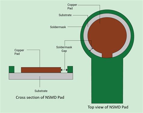
The soldermask is a thin layer of polymer that covers the copper traces on a PCB, leaving only the pads exposed where components will be soldered. Its purpose is to prevent solder bridges from forming between adjacent pads or traces during the soldering process. By pulling back the soldermask a certain distance from the pad edges, it creates a “window” that exposes more copper area for the solder to wet and form a strong mechanical and electrical connection.
Why is Soldermask Expansion Important?
Properly setting the soldermask expansion value is critical for several reasons:
- Solderability: A larger soldermask expansion exposes more copper area on the pads, allowing for better wetting of the solder and stronger solder joints. If the expansion is too small, there may not be enough exposed copper for the solder to adhere to, resulting in poor or unreliable solder connections.
- Manufacturing Yield: An appropriate soldermask expansion helps to accommodate normal variations in the soldermask alignment and etching process during PCB fabrication. If the expansion is too small, slight misalignments could cause the soldermask to partially or completely cover the pads, making it difficult or impossible to solder components. This leads to lower manufacturing yields and higher costs.
- Component Fit: The soldermask expansion also affects how well the component leads or terminals fit onto the pads. If the expansion is too large relative to the component size, there may be excessive space between the component and soldermask, allowing the component to shift or tombstone during soldering. On the other hand, if the expansion is too small, the component leads may overhang the soldermask and cause shorting or other issues.
Typical Soldermask Expansion Values
The appropriate soldermask expansion value depends on several factors, including the PCB manufacturing process, the component sizes and types, and the design requirements. However, there are some typical values that are commonly used as starting points:
| Component Type | Pad Size | Typical Expansion |
|---|---|---|
| Chip resistors, capacitors | 0402, 0603 | 0.05 – 0.1 mm |
| Chip resistors, capacitors | 0805, 1206 | 0.1 – 0.15 mm |
| SOT, QFP, SOIC | N/A | 0.15 – 0.25 mm |
| BGA, LGA | N/A | 0.25 – 0.5 mm |
These are just general guidelines, and the actual values used may vary depending on the specific design and manufacturing process. It’s always best to consult with the PCB fabricator and assembly house to determine the optimal soldermask expansion for a given project.
Designing with Soldermask Expansion
PCB Design Software Settings
Most PCB design software packages have built-in settings for specifying the soldermask expansion. This is typically done by defining a global setting that applies to all pads by default, and then overriding it for specific pads or component footprints as needed.
For example, in Altium Designer, the default soldermask expansion is set in the “Solder Mask Expansion” field under the “Pad” tab of the PCB Rules dialog. Individual pads can then have their own expansion values set in the Pad Properties dialog.
Other CAD packages may have similar settings located in different menus or dialogs, but the basic concept is the same. Consult the software documentation or support resources for specific instructions on how to set the soldermask expansion in a particular CAD tool.
Component Footprint Design
When creating or modifying component footprints for a PCB library, it’s important to consider the soldermask expansion and how it will affect the final assembled board. The footprint should be designed with appropriate pad sizes and shapes that will provide sufficient area for soldering while also accommodating the expected soldermask pullback.
Some general guidelines for footprint design with soldermask expansion in mind:
- Pad width and length should be large enough to allow for the desired expansion value without excessively reducing the solderable area. A common rule of thumb is to make the pad dimensions at least 0.2 mm larger than the minimum required for the component lead or terminal.
- For components with leads or pads that are very close together, such as fine-pitch QFPs or connectors, the soldermask expansion may need to be reduced to prevent solder bridges. In some cases, it may be necessary to use a “mask-defined pad” where the copper extends beyond the soldermask opening to provide additional clearance.
- Pads should be shaped and oriented to maximize the solderable area while minimizing the risk of tombstoning or shifting during reflow. Rectangular or oval pads are often preferred over round ones for this reason.
- The soldermask expansion should be consistent across all pads for a given component to ensure even soldering and prevent stresses that could cause reliability issues over time. Avoid using different expansion values for adjacent pads unless absolutely necessary.
Communicating with Manufacturers
When working with a PCB fabricator or assembly house, it’s important to clearly communicate the desired soldermask expansion values and any specific requirements for individual components or areas of the board. This can be done through notes or callouts on the fabrication drawings, or by providing a separate documentation file that lists the expansion values for each component or pad type.
Most manufacturers will have their own preferred or default soldermask expansion settings that they use for different types of components and PCB technologies. However, they should be able to accommodate specific requests from the designer as long as they are reasonable and within their process capabilities.
It’s always a good idea to discuss the soldermask expansion settings with the manufacturer early in the design process to ensure that they are achievable and will meet the project requirements. They may also be able to provide guidance or suggestions based on their experience and knowledge of the specific manufacturing processes and materials being used.

Common Issues and Solutions
Solder Bridging
One of the most common issues related to soldermask expansion is solder bridging, where solder inadvertently connects adjacent pads or traces due to insufficient clearance or masking. This can cause short circuits, signal integrity problems, and other functional issues with the assembled board.
Solder bridging can occur for several reasons, including:
- Soldermask expansion value is too small, allowing solder to wick or flow between pads
- Soldermask alignment or registration is poor, causing the openings to be misplaced or oversized
- Solder paste volume is too high, resulting in excess solder that can bridge between pads
- Reflow profile is incorrect, causing the solder to stay molten for too long or at too high a temperature
To prevent or mitigate solder bridging, some possible solutions include:
- Increase the soldermask expansion value to provide more clearance between pads
- Use a finer-pitch soldermask artwork to improve alignment and registration accuracy
- Reduce the solder paste volume or use a thinner stencil to apply less solder
- Optimize the reflow profile to minimize the time that the solder is molten and able to flow
- Use a solder mask-defined pad (SMD) instead of a copper-defined pad (NSMD) for critical components or areas
Tombstoning
Tombstoning, also known as drawbridging or Manhattan effect, is another common issue related to soldermask expansion. It occurs when a small SMD component, usually a chip resistor or capacitor, stands up on one end during soldering due to uneven heating or surface tension forces.
Tombstoning is more likely to occur when the soldermask expansion is too large relative to the component size, creating an excessive gap between the component and the soldermask that allows the component to tilt or lift off the pad. It can also be caused by uneven pad sizes or shapes, incorrect component placement, or poor reflow profile control.
To prevent tombstoning, some possible solutions include:
- Reduce the soldermask expansion to provide a tighter fit between the component and soldermask
- Ensure that the pad sizes and shapes are symmetric and balanced on both ends of the component
- Use a placement machine with vision alignment to accurately center the components on the pads
- Optimize the reflow profile to ensure even heating and minimize temperature gradients across the component
- Use a solder paste with higher viscosity or tackiness to help hold the component in place during reflow
Insufficient Wetting
Insufficient wetting occurs when the solder does not fully flow or adhere to the exposed copper on the pad, resulting in a weak or unreliable solder joint. This can be caused by several factors, including contamination, oxidation, or inadequate soldermask expansion.
If the soldermask expansion is too small, there may not be enough exposed copper area for the solder to wet and form a strong bond with the pad. This can lead to poor electrical and mechanical connections, as well as increased risk of fractures or failures under stress or thermal cycling.
To improve wetting and solder joint quality, some possible solutions include:
- Increase the soldermask expansion to expose more copper area on the pad
- Ensure that the pads are clean and free of contaminants or oxidation before applying solder paste
- Use a more active flux or higher-temperature solder alloy to promote wetting and flow
- Optimize the reflow profile to provide sufficient time and temperature for the solder to fully wet the pad
- Consider using a selective soldering process or hand soldering for critical components or areas

FAQ
What is the difference between soldermask expansion and pad size?
Pad size refers to the dimensions of the exposed copper area on a PCB where a component lead or terminal is soldered. Soldermask expansion is the additional area around the pad where the soldermask is pulled back to expose more copper for soldering. The pad size is determined by the component requirements and PCB design rules, while the soldermask expansion is set by the designer to ensure good solderability and manufacturability.
How do I choose the right soldermask expansion value for my design?
The appropriate soldermask expansion value depends on several factors, including the component size and type, PCB manufacturing process, and design requirements. As a general guideline, smaller components like chip resistors and capacitors typically use 0.05-0.15mm of expansion, while larger components like QFPs and BGAs may use 0.15-0.5mm or more. It’s always best to consult with the PCB fabricator and assembly house to determine the optimal value for a specific project.
Can I use different soldermask expansion values for different components on the same board?
Yes, it is possible to specify different soldermask expansion values for different components or areas of the PCB, depending on their specific requirements or constraints. However, it’s generally recommended to use a consistent value across the entire board whenever possible to simplify the manufacturing process and avoid potential issues with solder joint quality or reliability.
What happens if the soldermask expansion is too small or too large?
If the soldermask expansion is too small, there may not be enough exposed copper area for the solder to wet and form a strong connection, leading to poor solderability, weak joints, and potential reliability issues. If the expansion is too large, it can cause excessive space between the component and soldermask, allowing the component to shift or tombstone during reflow, or creating a risk of solder bridging between adjacent pads.
How do I communicate the soldermask expansion requirements to my PCB fabricator or assembly house?
The soldermask expansion requirements should be clearly specified in the PCB design files and fabrication drawings, either as a global setting or as specific values for individual components or areas. It’s also a good idea to provide a separate documentation file or note that lists the expansion values and any special requirements or considerations. Collaborating and consulting with the fabricator or assembler early in the design process can help ensure that the requirements are understood and achievable.


Leave a Reply