What is Solder Mask?
Solder mask, also known as solder resist or solder stop, is a thin layer of polymer applied to the copper traces of a printed circuit board (PCB). Its primary purpose is to protect the copper traces from oxidation, prevent solder bridges from forming between closely spaced pads, and provide electrical insulation. Solder mask also serves as a protective barrier against environmental factors such as moisture, dust, and other contaminants.
Types of Solder Mask
There are two main types of solder mask materials:
-
Liquid Photoimageable Solder Mask (LPSM): This type of solder mask is applied as a liquid and then exposed to UV light through a photographic film. The exposed areas harden, while the unexposed areas are washed away during development. LPSM is the most common type of solder mask used in PCB manufacturing.
-
Dry Film Solder Mask (DFSM): This type of solder mask is supplied as a dry film that is laminated onto the PCB surface. It is then exposed to UV light and developed, similar to the LPSM process. DFSM is less common than LPSM but is still used in some applications.
Solder Mask Material Properties
The choice of solder mask material depends on various factors, including the PCB’s intended application, environmental conditions, and manufacturing process. Some essential properties to consider when selecting a solder mask material include:
Electrical Properties
- Dielectric Strength: The ability of the solder mask to withstand high voltage without breaking down. A higher dielectric strength ensures better insulation between conductors.
- Surface Resistance: The resistance of the solder mask surface to the flow of electrical current. Higher surface resistance helps prevent leakage currents and short circuits.
Mechanical Properties
- Adhesion: The ability of the solder mask to adhere to the PCB surface and copper traces. Good adhesion prevents delamination and ensures long-term reliability.
- Flexibility: The ability of the solder mask to withstand bending and flexing without cracking or peeling. This is particularly important for flexible PCBs.
Chemical Properties
- Resistance to Solvents: The ability of the solder mask to withstand exposure to various solvents used in PCB Cleaning and manufacturing processes.
- Resistance to Acids and Alkalines: The ability of the solder mask to withstand exposure to acidic and alkaline solutions, which may be present in some manufacturing processes or operating environments.
Thermal Properties
- Glass Transition Temperature (Tg): The temperature at which the solder mask material transitions from a rigid, glassy state to a softer, rubbery state. A higher Tg ensures better thermal stability and resistance to high-temperature processes such as soldering.
- Coefficient of Thermal Expansion (CTE): The rate at which the solder mask material expands and contracts with changes in temperature. A CTE that closely matches that of the PCB substrate helps prevent stress and warping during temperature cycling.

Solder Mask Application Process
The solder mask application process typically involves the following steps:
-
Cleaning: The PCB surface is cleaned to remove any contaminants or residues that may affect solder mask adhesion.
-
Application: The solder mask material is applied to the PCB surface using either screen printing (for LPSM) or lamination (for DFSM).
-
Exposure: The solder mask is exposed to UV light through a photographic film or phototool. The exposed areas of the solder mask harden, while the unexposed areas remain soluble.
-
Development: The unexposed areas of the solder mask are removed using a chemical developer, leaving behind the hardened solder mask pattern.
-
Curing: The solder mask is fully cured through a combination of UV exposure and thermal baking to achieve its final properties.

Solder Mask Colors
Solder mask is available in a variety of colors, with green being the most common. Other popular colors include blue, red, yellow, black, and white. The choice of color is primarily aesthetic but can also serve functional purposes, such as:
- Improving contrast for better visual inspection
- Indicating different PCB versions or revisions
- Enhancing heat dissipation (e.g., black solder mask)
- Providing UV protection (e.g., opaque colors)

Solder Mask Design Considerations
When designing a PCB with solder mask, several factors must be considered to ensure optimal performance and manufacturability:
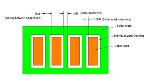
Solder Mask Clearance
Solder mask clearance refers to the distance between the edge of a copper pad and the edge of the solder mask opening. Adequate clearance is essential to ensure proper solder wetting and prevent solder mask from encroaching on the pad area. The minimum solder mask clearance depends on the PCB manufacturer’s capabilities and the solder mask material used, but a typical value is 0.1 mm (4 mil).
Solder Mask Sliver
A solder mask sliver is a thin strip of solder mask between two closely spaced copper features, such as pads or traces. If the sliver is too narrow, it may break off during manufacturing or use, leading to short circuits or other defects. To avoid this, PCB designers should adhere to the manufacturer’s minimum solder mask sliver width guidelines, which typically range from 0.1 mm to 0.15 mm (4 to 6 mil).
Solder Mask Expansion
Solder mask expansion refers to the enlargement of solder mask openings to accommodate the solder mask registration tolerance. This ensures that the solder mask opening is always larger than the copper pad, even if there is a slight misalignment during the solder mask application process. The amount of solder mask expansion required depends on the PCB manufacturer’s capabilities and the solder mask material used, but a typical value is 0.05 mm to 0.075 mm (2 to 3 mil) per side.
Solder mask dams
Solder mask dams are thin strips of solder mask placed between adjacent copper pads or traces to prevent solder bridging. They are particularly useful in fine-pitch components or high-density PCB designs. The width of the solder mask dam should be sufficient to provide adequate insulation and prevent solder from flowing between the pads.
Solder Mask and Surface Finish
The choice of surface finish can affect the performance and appearance of the solder mask. Some common surface finishes used with solder mask include:
- Hot Air Solder Leveling (HASL): A tin-lead alloy is applied to the exposed copper pads and then leveled using hot air. HASL provides good solderability but can result in an uneven surface and may not be suitable for fine-pitch components.
- Electroless Nickel Immersion Gold (ENIG): A layer of nickel is deposited on the exposed copper pads, followed by a thin layer of gold. ENIG provides excellent solderability, flatness, and shelf life but can be more expensive than other surface finishes.
- Immersion Tin (IT): A thin layer of tin is deposited on the exposed copper pads. IT provides good solderability and is less expensive than ENIG but has a shorter shelf life.
- Immersion Silver (IS): A thin layer of silver is deposited on the exposed copper pads. IS provides good solderability and is less expensive than ENIG but may tarnish over time.
The choice of surface finish should be based on the specific requirements of the PCB, such as solderability, shelf life, and cost.
Solder Mask and PCB assembly
Solder mask plays a crucial role in the PCB assembly process, particularly during solder paste printing and component placement.
Solder Paste Printing
Solder paste is applied to the exposed copper pads through a stencil using a screen printing process. The solder mask acts as a barrier, preventing solder paste from spreading onto the non-pad areas of the PCB. This ensures that the solder paste is deposited only where it is needed, reducing the risk of short circuits and other defects.
Component Placement
After solder paste printing, the components are placed onto the PCB using automated pick-and-place machines. The solder mask helps guide the placement of the components by providing a clear visual contrast between the copper pads and the surrounding areas. This ensures accurate component positioning and reduces the risk of misalignment.
Solder Mask Defects and Quality Control
Several defects can occur during the solder mask application process, which can affect the performance and reliability of the PCB. Some common solder mask defects include:
- Pinholes: Small holes or voids in the solder mask that expose the underlying copper. Pinholes can lead to short circuits, corrosion, or other reliability issues.
- Solder Mask Residue: Incomplete removal of unexposed solder mask during development, leaving residue on the copper pads or in the solder mask openings. Residue can affect solderability and lead to poor solder joint formation.
- Solder Mask Misregistration: Misalignment between the solder mask and the copper features, resulting in exposed copper or solder mask encroaching on the pad area. Misregistration can affect solderability and lead to short circuits or other defects.
- Solder Mask Blistering: Formation of bubbles or blisters in the solder mask due to improper curing or contamination. Blistering can affect the insulation properties of the solder mask and lead to reliability issues.
To ensure the quality of the solder mask application, PCB manufacturers employ various quality control methods, such as:
- Visual inspection using automated optical inspection (AOI) systems or manual microscopic examination
- Electrical testing to verify insulation resistance and dielectric strength
- Adhesion testing to ensure proper bonding between the solder mask and the PCB surface
- Solderability testing to validate the wetting properties of the exposed copper pads
By implementing strict quality control measures, PCB manufacturers can minimize the occurrence of solder mask defects and ensure the overall reliability of the finished PCB.
Frequently Asked Questions (FAQ)
-
What is the difference between solder mask and conformal coating?
Solder mask is applied to the PCB surface before assembly and serves to protect the copper traces, prevent solder bridging, and provide electrical insulation. Conformal coating, on the other hand, is applied after assembly and provides additional protection against moisture, dust, and other environmental factors. Conformal coating covers the entire PCB surface, including components, while solder mask only covers the non-pad areas. -
Can solder mask be removed?
Yes, solder mask can be removed using various methods, such as chemical stripping, laser ablation, or mechanical abrasion. However, removing solder mask should only be done when absolutely necessary, as it can damage the underlying copper traces and affect the overall reliability of the PCB. -
What is the typical thickness of solder mask?
The typical thickness of solder mask ranges from 0.01 mm to 0.03 mm (0.4 to 1.2 mil), depending on the application and the solder mask material used. Thicker solder mask provides better insulation and protection but may affect the fine-pitch capability of the PCB. -
Can solder mask be applied to both sides of the PCB?
Yes, solder mask can be applied to both sides of the PCB, depending on the design requirements. In fact, most PCBs have solder mask on both sides to protect the copper traces and provide insulation. However, some specialized PCBs, such as those used in high-frequency applications, may have solder mask on only one side to minimize the dielectric effect. -
How does solder mask affect the impedance of the PCB traces?
Solder mask has a dielectric constant that is higher than that of air, which can affect the impedance of the PCB traces. The presence of solder mask increases the capacitance between the traces and the ground plane, leading to a decrease in impedance. This effect is more pronounced in high-frequency PCBs, where impedance control is critical. To compensate for the effect of solder mask, PCB designers may need to adjust the trace width and spacing to maintain the desired impedance.
In conclusion, solder mask is an essential material in PCB manufacturing that serves to protect the copper traces, prevent solder bridging, and provide electrical insulation. The choice of solder mask material and color depends on various factors, such as the intended application, environmental conditions, and manufacturing process. PCB designers must consider several factors, such as solder mask clearance, sliver, expansion, and dams, to ensure optimal performance and manufacturability. Solder mask plays a crucial role in the PCB assembly process and is subject to various defects that can affect the reliability of the finished PCB. By understanding the properties, application process, and design considerations of solder mask, PCB designers and manufacturers can ensure the production of high-quality, reliable PCBs.


Leave a Reply