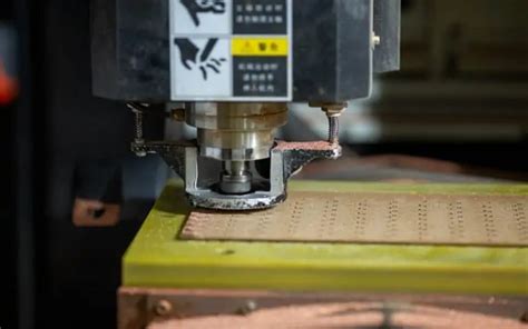
Introduction to PCB Panelization
PCB panelization is the process of arranging multiple printed Circuit Board Designs on a single panel for manufacturing. This technique is commonly used in PCB Fabrication to increase production efficiency and reduce costs. By grouping several PCBs together, manufacturers can optimize material usage, minimize handling, and streamline the assembly process.
Benefits of PCB Panelization
- Cost reduction: Panelizing PCBs allows for the production of multiple boards in a single run, reducing setup time and material waste.
- Increased efficiency: Handling a panel of PCBs is faster and more efficient than dealing with individual boards.
- Improved consistency: Panelization ensures that all boards in a panel are subjected to the same manufacturing conditions, resulting in more consistent quality.
- Simplified assembly: Panelized PCBs can be easily separated after manufacturing, making the assembly process more straightforward.
PCB Panelization Software
To effectively panelize PCBs, designers and manufacturers rely on specialized software tools. These tools allow users to arrange multiple PCB Designs on a single panel, define the spacing between boards, and add necessary features such as Fiducial Markers and tooling holes.
Popular PCB Panelization Software
| Software | Description | Key Features |
|---|---|---|
| Altium Designer | A comprehensive PCB design software with built-in panelization tools. | – Automatic and manual panelization options – Support for complex panel shapes – Customizable panel reports |
| Mentor Graphics Xpedition | A powerful PCB design platform with advanced panelization capabilities. | – Drag-and-drop panel creation – Real-time panel optimization – Automatic panel validation |
| Zuken CR-8000 | A complete PCB design solution with integrated panelization functionality. | – Automatic panel generation – Support for mixed-size panels – Customizable panel templates |
Factors to Consider When Choosing PCB Panelization Software
- Compatibility with existing PCB design tools
- Ease of use and learning curve
- Automated features for panel optimization
- Support for various panel shapes and sizes
- Integration with manufacturing processes

PCB Panelization Techniques
There are several techniques used in PCB panelization, each with its own advantages and considerations.
Tab Routing
Tab routing involves connecting individual PCBs with thin tabs that can be easily broken after manufacturing. This technique is simple and cost-effective but may require manual separation of the boards.
V-Scoring
V-scoring uses a V-shaped groove cut along the edges of each PCB, allowing for easy separation. This method provides a clean break but may weaken the panel structure.
Perforated Routing
Perforated routing creates a series of small holes along the edges of each PCB, enabling easy separation. This technique offers a balance between strength and ease of separation but may require special tooling.
Snap-Apart Routing
Snap-apart routing uses a combination of tab routing and perforated routing to create a panel that can be easily snapped apart. This method provides a good compromise between strength and ease of separation.

Best Practices for PCB Panelization
To ensure successful PCB panelization, consider the following best practices:
- Optimize panel layout for maximum material utilization
- Include fiducial markers for accurate alignment during assembly
- Use consistent spacing between boards to ensure proper separation
- Add tooling holes for handling and registration during manufacturing
- Verify panel design with the manufacturer before production

Frequently Asked Questions (FAQ)
1. What is the optimal panel size for PCB manufacturing?
The optimal panel size depends on the specific requirements of the project and the capabilities of the manufacturing facility. Common panel sizes include 18″ x 24″, 21″ x 24″, and 24″ x 36″. Consult with your manufacturer to determine the best panel size for your needs.
2. How much space should be left between PCBs on a panel?
The spacing between PCBs on a panel, also known as the “web,” typically ranges from 0.1″ to 0.2″. The exact spacing depends on the panelization technique used and the requirements of the manufacturing process. It is essential to maintain consistent spacing to ensure proper separation of the boards.
3. Can different PCB designs be panelized together?
Yes, different PCB designs can be panelized together on the same panel, provided they have similar specifications such as thickness, copper weight, and surface finish. This technique, known as “mixed-panel” or “multi-array” panelization, can help optimize material usage and reduce production costs.
4. What are fiducial markers, and why are they important in PCB panelization?
Fiducial markers are small, precisely placed features on a PCB panel that serve as reference points for alignment during manufacturing. They ensure accurate positioning of the panel during the assembly process, particularly for automated pick-and-place machines. Fiducial markers are crucial for maintaining consistency and quality in PCB production.
5. How can I ensure my PCB panel design is compatible with the manufacturer’s requirements?
To ensure compatibility with the manufacturer’s requirements, it is essential to communicate your design intent and specifications clearly. Provide detailed panel drawings, including dimensions, panelization technique, and any special requirements. It is also advisable to request a design review or feedback from the manufacturer before finalizing your panel design.
Conclusion
PCB panelization is a crucial aspect of PCB manufacturing that enables cost-effective and efficient production. By utilizing specialized software tools and appropriate panelization techniques, designers and manufacturers can optimize panel layouts, minimize material waste, and streamline the assembly process.
When considering PCB panelization, it is essential to choose software that is compatible with existing design tools, offers automated optimization features, and supports various panel shapes and sizes. Additionally, following best practices such as optimizing panel layout, including fiducial markers, and maintaining consistent spacing between boards can help ensure successful panelization.
By understanding the benefits, techniques, and best practices of PCB panelization, designers and manufacturers can make informed decisions that lead to cost savings, improved efficiency, and higher-quality PCB production.


Leave a Reply