Introduction to Small Scale PCB Production
Printed circuit boards (PCBs) are essential components in almost all modern electronics. While large scale manufacturing has made PCBs very inexpensive, producing prototypes and small batches can still be quite costly using traditional fabrication techniques. As the popularity of hardware startups and DIY electronics has grown, so has the need for more accessible small run PCB options.
In this guide, we’ll look at the key considerations around low volume PCB production. We’ll examine the available methods and how to choose the right one for your project based on factors like:
- Quantity needed
- Budget
- Timeframe
- Design complexity
We’ll also review tips for optimizing your boards for manufacturability when you’re designing for short runs.
Overview of Small Scale PCB Production Methods
There are three main routes available for getting a small number of PCBs produced:
Professional Fabrication
This is using a traditional PCB manufacturer to produce your boards. Most fabricators offer discounts at higher quantities, but will still produce runs as small as 10-50 boards.
Batching Services
These act as a middleman, aggregating small orders together to get bulk discounts from fabricators. This makes small runs cost effective but adds time and logistics.
DIY Methods
DIY PCB production using CNC milling, lasers, or etching allows making boards yourself with reduced costs but higher effort.
Let’s look at each of these options in more detail:
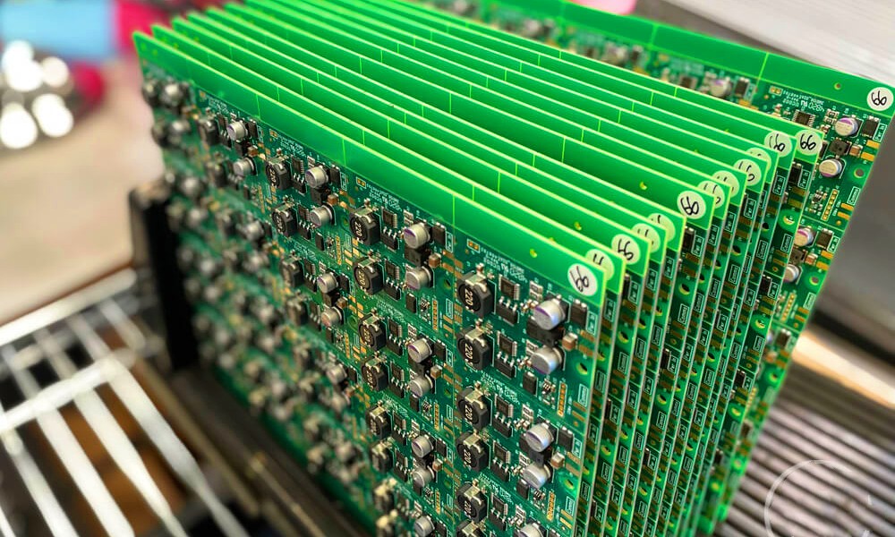
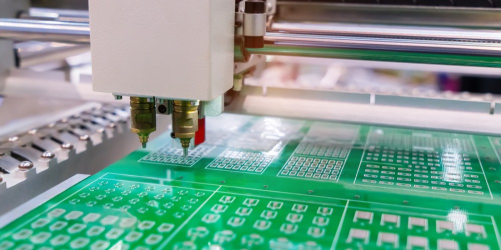
Professional PCB Fabrication
The traditional approach is to work directly with a PCB manufacturer. Most fabricators offer discounts at higher volumes but can still produce very small batches.
When using a pro fabricator, you’ll generally go through the following process:
- Design – Create schematics and board layout in CAD software like Eagle, KiCad, Altium etc.
- Gerber Files – Export Gerber and drill files for manufacturing. Include any instructions.
- Quote – Upload to fabricator’s website for an instant online quote.
- Order – Place order and pay for boards to be made. Lead time is usually ~10 days.
- Manufacturing – Fabricator creates your boards.
- Shipping – Boards are shipped to you.
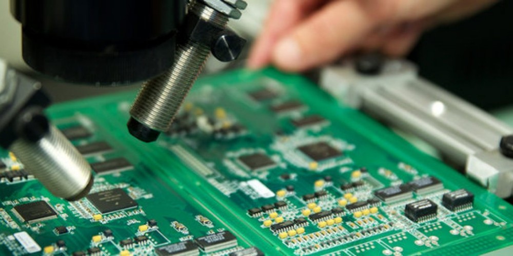
- Assembly – Solder components onto the manufactured PCB.
Some major advantages of professional fabrication:
- Very high reliability and quality
- Wide range of board capabilities and sizes
- Fast turnaround; boards in ~10 days
- No need for any equipment or materials
The main disadvantages:
- High NRE (non-recurring engineering) costs for low volumes
- Often has larger minimum order quantities (MOQs)
For very complex or high density designs, professional fabrication is hard to beat. But for simpler boards, the setup costs can make it expensive for prototyping.
PCB Batching Services
To reduce the costs of small scale fabrication, PCB batching services aggregate together orders from multiple customers. By producing many customer designs simultaneously, they achieve bulk pricing from the fabricators.
The process of using a PCB batching service involves:
- Upload your Gerber design files
- Select options like quantity, layers, solder mask, etc
- Pay for your boards to be queued for fabrication
- Your boards are grouped with other user designs
- All designs are manufactured as a single large board
- Batching company breaks apart and ships individual boards
Lead times are slightly longer than working with a fabricator directly, often ~14-21 days. But in return you save on NRE costs through the combined bulk orders.
Some of the most popular PCB batching services:
- PCBWay
- JLCPCB
- OSH Park
- Aisler
Batching makes the setup costs of PCB production accessible for prototyping and medium batches between 10-100 boards. But for very low or very high quantities, professional fabricators are often still better in terms of cost and lead time.
DIY PCB Fabrication
If you need just a handful of boards, DIY fabrication can be an economical option. Producing boards yourself drastically reduces setup costs and minimum order quantities.
Some common DIY methods include:
Milling: CNC milling a copper clad laminate to isolate traces based on your layout.
Laser: Using a laser cutter to selectively ablate copper on FR-4 laminate.
Etching: Chemically etching away copper on a blank PCB to leave just the desired conductor pattern.
DIY fabrication requires some investment in equipment and materials. But in return you get:
- Ultra low volume capability – make even just a single board
- Low NRE costs for prototyping
- Very fast fabrication time
The tradeoff is that DIY techniques have more limited capabilities than professional processes. But for simple boards with large features, DIY can be a great source of fast, cheap prototypes.
Choosing the Right PCB Production Method
With the various options covered, let’s look at how to select the optimal technique based on your specific project. The main factors to consider are:
Required Quantity
What’s the number of boards needed? Different methods have different ideal quantities:
- Professional fabrication = 10-500+
- Batching services = 10-100
- DIY = 1-10
So match your method to the quantity you actually need.
Budget
DIY has the lowest costs but higher startup cost for equipment. Professional can be expensive for low volumes. Batching hits a nice middle ground.
Timeframe
DIY is extremely fast, under 1-2 days. Batching is medium turnaround, ~2 weeks. Professional is speedy too at ~10 days.
Design Complexity
DIY works best for simple designs with large traces. Professional houses handle much more density and complexity.
Available Resources
If you already have a CNC mill or laser cutter, doing DIY will save purchase costs. Without existing equipment, outsourcing fabrication is easiest.
Based on factors like these, you can select the optimal production method for your particular small run PCB needs.
Here’s a quick comparison table of the different options:
| Method | Quantities | Lead Time | Cost Per Board | Complexity | Equipment Needed |
|---|---|---|---|---|---|
| Professional | 10-500+ | ~10 days | $$$ at low volumes | High | None |
| Batching Service | 10-100 | ~14-21 days | $$ | Medium-high | None |
| DIY | 1-10 | < 2 days | $ | Low | DIY tools |
Optimizing Designs for Small Batch PCB Production
To get the most success out of low volume PCB production, you can optimize your circuit designs for manufacturability. Here are some key design tips:
Allow for Larger Traces and Spaces
The DIY methods have lower resolution than professional processes. So increase trace widths and clearances to at least 10 mils.
Avoid Tiny Vias
Small vias are harder to properly fill with plating. Keep vias larger than 0.4 mm diameter if possible.
Reduce Hole Sizes
For DIY drilling, smaller holes are easier to produce than larger ones. When possible, use holes of 0.6mm or less.
Allow for Panelization
Include mouse bites or v-scores in your design to allow for breakout tabs when fabricated on panels.
Watch High Frequency Layout
DIY processes can’t match pro grade dielectrics. Keep controlled impedances loose if possible.
minimize layers
Stick to 1 or 2 layer designs. More layers are challenging for DIY fabrication.
Design Panel Supports
Include fiducials and tooling holes for proper panel alignment and breakout.
Following these guidelines will maximize yield and reduce issues when making your own boards in low volumes.
Conclusion
Small run PCB production opens up professional grade circuit manufacturing even for prototypes, hobbyists, and education. The choice between DIY fabrication, batching services, and professional outsourcing depends on your specific needs and resources. Optimizing designs for manufacturability helps ensure success. But with careful planning, even complex boards can be produced affordably at low scale.
Frequently Asked Questions
What are typical minimum order quantities for small scale PCB production?
For professional fabrication, minimums are often around 10-50 boards but can be as low as 5. Batching combines orders so can go down to just 1-5 boards. DIY techniques have no minimum.
How do the costs compare between DIY, batching, and professional fabrication?
DIY has the lowest material costs but higher equipment investment. Batching is moderately priced but saves on NRE costs. Professional is most expensive for super low quantities but has volume discounts.
Is surface mount assembly possible with hobbyist PCB production?
It’s generally recommended to stick to through hole components when doing DIY assembly. Some hobbyists have success with hand soldering or reflowing simple SMT parts. Complex BGAs are very difficult with DIY equipment.
Can you make multi-layer boards at home?
It’s possible but challenging. Laser ablation and CNC milling can be used to selectively expose internal layers. But registration and drilling for vias gets tricky. 2 layers is much more consistently successful.
How many times can I re-work a DIY PCB?
The home etching and milling process is not nearly as robust as professional fabrication. Expect to only get 1-2 assemblies out of a DIY board before quality degrades too far.


Leave a Reply