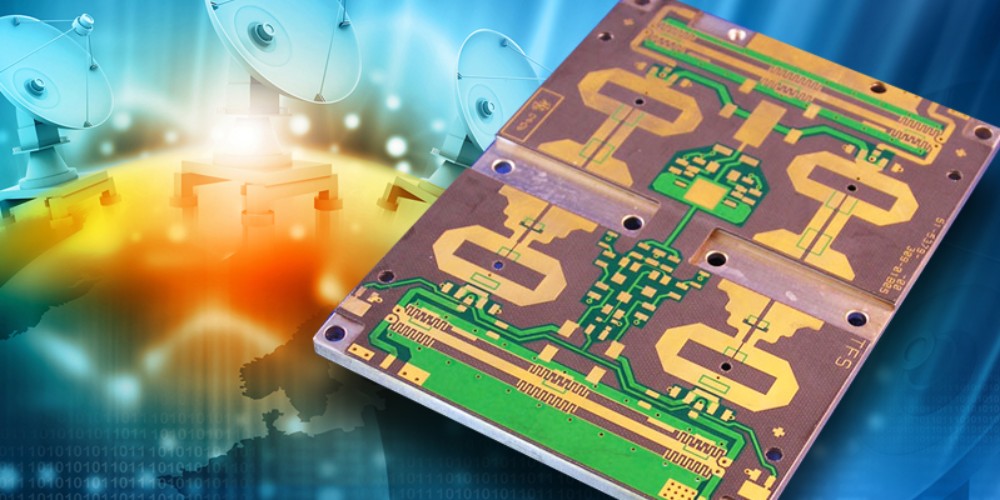
Introduction
Printed circuit boards (PCBs) that operate at radio frequencies (RF) require special design considerations to ensure proper functioning of high-frequency circuits. Choosing the right RF PCB manufacturer is crucial for building complex wireless systems and products involving technologies like 5G, Wi-Fi, Bluetooth, GPS and more. This article provides a comprehensive guide on selecting an ideal RF PCB production partner for your specific application needs.
Key Factors to Consider in an RF PCB Manufacturer
Experience with High-Frequency PCBs
Look for manufacturers with proven expertise in RF PCBs used in cellular, microwave, radar and other wireless applications. They must demonstrate in-depth knowledge of designing for high frequencies, impedance control, crosstalk minimization and signal integrity. Prefer suppliers regularly manufacturing PCBs for over 5Ghz frequencies.
Specialized RF Materials and Stackup
The PCB substrate material and layer stackup are critical for RF performance. Choose a fabricator with access to top-quality RF materials like Rogers and Taconic laminates and expertise in selecting suitable dielectrics, copper weights, finishes, etc. for your design.
Precision Impedance Control and Matching
Maintaining tight impedance tolerances is vital for RF PCBs. Select a manufacturer equipped with processes like micro-etching capability to hold tight impedance across traces, tracks and other features. Also, the accuracy of impedance tuning structures like tapers is important.
Skilled Engineers and Quality Processes
Look for knowledgeable RF engineers on staff who can provide design rule checking and advise on optimizations. Make sure the company follows consistent high-quality processes for fabrication, testing and inspection using automation where possible. They should be certified to quality standards like ISO 9001.
Comprehensive Testing and Measurement
RF testing requires specialized equipment like vector network analyzers. Choose a supplier with full in-house testing capabilities for parameters like insertion loss, VSWR, return loss and phase. This enables identifying issues early and verifying adherence to your specs.
Advanced Technology and Manufacturing Capability
The latest manufacturing equipment and technologies are essential for complex RF PCBs. Look for builders with cutting-edge drilling, imaging, etching and routing capabilities. Multilayer boards with high layer counts, fine features, blind/buried vias, etc. require advanced fabrication techniques.
Prototyping Support and Fast Turnarounds
The ability to quickly iterate prototypes is helpful during RF product development. Choose a supplier with quick-turn fabrication of short prototype runs and pre-production small batches. This allows swift design verification and refinement before final volume production.
Experience with End-User Applications
Preferred RF PCB partners have experience manufacturing for similar end-use cases as your product. For example, expertise in boards for cellular base stations if you are building 5G equipment. Relevant application knowledge helps in design-for-manufacturing.
RF PCB Materials Used By Leading Manufacturers
RF PCB substrates play a major role in circuit performance. Here are some of the popular materials used by top manufacturers:
FR-4
The economical go-to material for many PCBs. Different grades of FR-4 laminates are available, some optimized for high frequencies up to a few GHz.
High-Frequency Laminates
Premium materials like Rogers RO4000 and RO3000 series cater to high-speed RF applications. Other popular options are Taconic’s TLY and TacLam laminates.
Ceramic Filled PTFE Composites
Materials like Rogers RT/duroid 6000 incorporate ceramic filler in PTFE fluoropolymer matrix for excellent high-frequency performance. Low loss, tight tolerance and stability make them suitable for mmWave applications.
PTFE Based Substrates
Polytetrafluoroethylene (PTFE) substrates like Rogers 4003C provide tight dielectric constant tolerance, low loss and low moisture absorption for frequencies over 10 GHz.
High Frequency LCP
Liquid Crystal Polymer (LCP) laminates like Rogers ULTRALAM 3850 show consistent electrical performance over wide frequency ranges. LCP is also used in flex circuits for RF applications.
Quartz and Glass
Quartz and glass laminates offer extremely low loss at high frequencies and stable dielectric properties. But they are more expensive than conventional PCB substrates.
RF PCB Manufacturing Capabilities Offered by Leading Companies
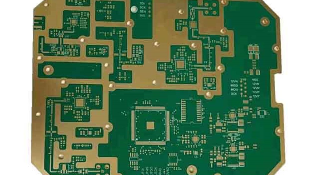
Here are some of the key manufacturing capabilities offered by top RF PCB fabrication suppliers:
Multilayer High Density Interconnects (HDI)
Ability to produce multilayer boards with stacked microvias and fine lines/spaces enabling high interconnect density. This allows integrating more components and routing complex circuitry.
Blind and Buried Vias
Blind/buried vias connect inner layers without drilling through the entire PCB stackup. This helps shorten traces for better high-frequency response and component packing.
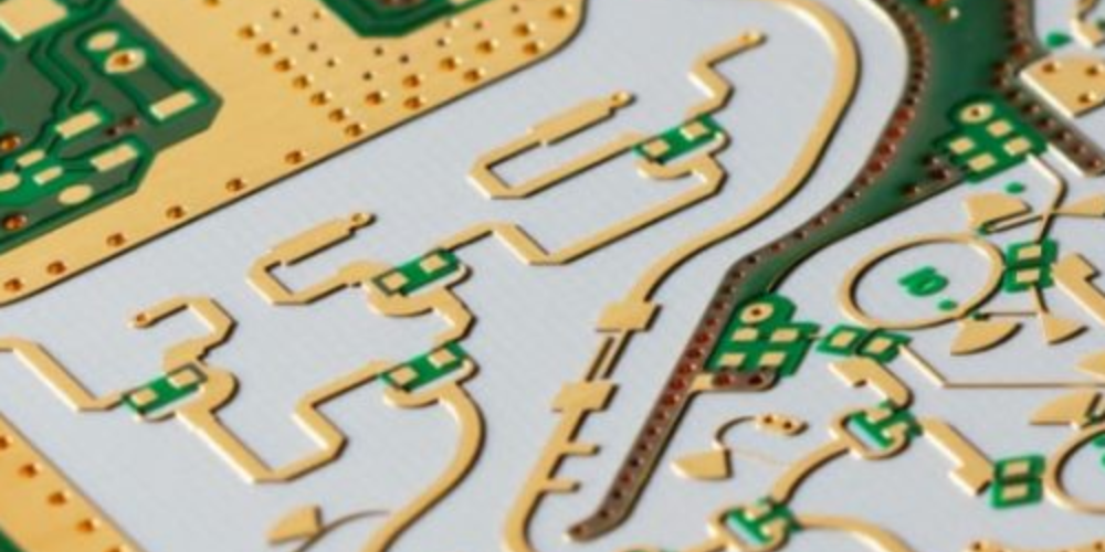
Fine Line PCBs
PCB features under 6 mil line width and spacing to build compact RF circuits and integrate more functionality. Requires excellent imaging and etching techniques.
Laser Drilling
Laser drilling forms small diameter holes with tight tolerance ideal for HDI boards. It also allows drilling non-circular shaped vias.
Sequential Lamination
Building up PCB layer stack with multiple lamination cycles. Useful for embedding components inside the board and adding layers only where needed.
Panel Plating
Plating large panel sizes for better process control and consistency across PCB batches compared to standard pattern plating.
Automated Optical Inspection (AOI)
Using AOI machines to check PCB quality and identify defects during fabrication improves process control and early problem detection.
Controlled Impedance Trace Routing
Capability to design impedance matched traces and structures as required by RF application circuits.
Rigid-Flex PCBs
Combining rigid and flexible substrates in one PCB allows 3D configuration and integration of disparate components into a compact, optimized form.
FQA
What are some challenges in manufacturing RF PCBs?
Some key challenges include maintaining tight impedance tolerances, dealing with high-frequency signal losses, ensuring consistent dielectric properties, fabricating multilayer boards without affecting performance, minimizing crosstalk and EMI, etc.
How is RF PCB design different from regular PCBs?
RF design requires attention to impedance control, proper grounding, dealing with radiation losses, high-speed layout techniques, simulation of various parameters like S-parameters, thermal analysis for power circuitry etc.
What testing should be done to verify RF PCB performance?
Essential tests include impedance, insertion loss, VSWR measurements, power handling tests; for wireless boards additional OTA (over-the-air) testing is required.
How can I ensure signal integrity in my high-frequency PCB?
Choose suitable RF materials, use impedance matched traces, provide adequate ground planes, include ground vias along signal traces, minimize abrupt direction changes in traces, avoid shortcuts between reference planes etc.
What fabrication tolerances should I expect for RF PCBs?
You can expect impedance tolerances within 5-10%, dielectric constant tolerance +/-2-3%, layer to layer registration around 4-6 mils and features/spaces in 2-4 mil range from leading manufacturers.
Conclusion
Choosing the right RF PCB partner requires careful evaluation of their material expertise, manufacturing capabilities, quality systems, testing facilities, engineering resources and application experience. I hope this guide summarizes the key factors and technologies to look for when selecting a fabrication supplier for your wireless or high-frequency PCB product development. Leveraging an experienced RF PCB manufacturer with robust processes can help mitigate design risks and ensure your product performs as intended in the target frequency range.


Leave a Reply