Understanding Solder Mask and Its Importance
Solder mask, also known as solder resist or solder stop, is a thin protective layer applied to the copper traces of a printed circuit board (PCB). Its primary purpose is to prevent solder from bridging between adjacent pads or tracks during the soldering process. Solder mask also provides protection against oxidation and contamination of the copper traces, improving the overall reliability and longevity of the PCB.
Types of Solder Mask
There are two main types of solder mask:
-
Liquid Photoimageable Solder Mask (LPSM): This type of solder mask is applied as a liquid and then exposed to UV light through a photographic film. The exposed areas harden, while the unexposed areas are washed away during development.
-
Dry Film Solder Mask (DFSM): This type of solder mask is applied as a dry film and then exposed to UV light through a photographic film. The exposed areas remain intact, while the unexposed areas are removed during development.
Solder Mask Properties
A high-quality solder mask should possess the following properties:
- Good adhesion to the copper surface
- High resistance to solder heat and chemicals
- Excellent electrical insulation
- Smooth and uniform surface finish
- Adequate thickness (typically 0.5-1.0 mils)
Causes of Solder Mask Bridge Breaking Off
Despite the importance of solder mask in PCB manufacturing, there are several reasons why solder mask bridges may break off, leading to potential issues such as short circuits, signal integrity problems, and reduced reliability. Let’s explore the main causes of solder mask bridge breakoff.
1. Improper Solder Mask Application
One of the primary reasons for solder mask bridge breakoff is improper application of the solder mask material. This can occur due to various factors, such as:
-
Incorrect solder mask thickness: If the solder mask is applied too thinly, it may not provide adequate protection and may be more prone to breaking off. Conversely, if the solder mask is applied too thickly, it can lead to poor adhesion and increased stress on the copper traces.
-
Inadequate curing: If the solder mask is not properly cured, it may not achieve the necessary mechanical and chemical properties, making it more susceptible to breaking off during the soldering process or in the field.
-
Contamination: Any contamination on the copper surface or in the solder mask material can interfere with proper adhesion and lead to solder mask bridge breakoff.
2. PCB Design Issues
Certain aspects of PCB design can contribute to solder mask bridge breakoff:
-
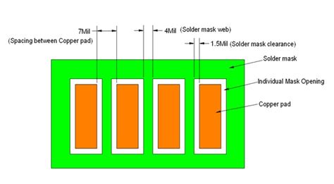
Insufficient solder mask clearance: If the solder mask openings around pads and traces are too small, there may not be enough space for the solder mask to adhere properly, leading to increased stress and potential breakoff.
-
Acute angles in copper traces: Sharp angles in copper traces can create stress concentrations, making the solder mask more likely to break off in those areas.
-
High-density layouts: As PCB designs become more complex and densely populated, the spacing between pads and traces decreases, making it more challenging to achieve reliable solder mask coverage and increasing the risk of bridge breakoff.
3. Thermal Stress
During the soldering process, PCBs are subjected to high temperatures, which can cause thermal stress on the solder mask and copper traces. If the solder mask and copper have different coefficients of thermal expansion (CTE), this can lead to stress buildup and potential solder mask bridge breakoff.
Factors that can contribute to thermal stress include:
-
Excessive soldering temperatures: If the soldering temperature is too high or the exposure time is too long, it can cause the solder mask to degrade or break off.
-
Rapid temperature changes: Sudden temperature fluctuations, such as those experienced during reflow soldering or thermal cycling, can cause the solder mask and copper to expand and contract at different rates, leading to stress and potential breakoff.
4. Mechanical Stress
Mechanical stress can also contribute to solder mask bridge breakoff, particularly during handling, assembly, or in the field. Some sources of mechanical stress include:
-
Bending or flexing of the PCB: If the PCB is subjected to excessive bending or flexing, it can cause the solder mask to crack or break off, especially in areas with high-stress concentrations.
-
Vibration and shock: Exposure to vibration or shock during transportation, assembly, or in the field can cause the solder mask to break off, particularly if there are pre-existing weak points or defects.
-
Improper handling: Rough handling or misalignment during assembly can lead to mechanical damage and solder mask bridge breakoff.
5. Environmental Factors
Environmental factors can also play a role in solder mask bridge breakoff, particularly over the long term. Some key environmental factors include:
-
Moisture and humidity: Exposure to high humidity or moisture can cause the solder mask to absorb water, leading to swelling, loss of adhesion, and potential breakoff.
-
Chemical exposure: Exposure to certain chemicals, such as cleaning agents or flux residues, can degrade the solder mask and make it more susceptible to breaking off.
-
UV exposure: Prolonged exposure to UV light can cause the solder mask to become brittle and more prone to cracking or breaking off.

Preventing Solder Mask Bridge Breakoff
To minimize the risk of solder mask bridge breakoff, several strategies can be employed during PCB design, manufacturing, and assembly:
-
Proper solder mask selection: Choose a high-quality solder mask material that is compatible with the specific requirements of the PCB, such as the soldering process, operating environment, and expected lifetime.
-
Optimal solder mask application: Ensure that the solder mask is applied with the correct thickness, uniformity, and curing conditions to achieve good adhesion and mechanical properties.
-
PCB design optimization: Incorporate design features that minimize stress on the solder mask, such as adequate solder mask clearance, avoiding acute angles in copper traces, and using teardrops or reinforced pads where necessary.
-
Controlled soldering process: Use appropriate soldering temperatures and exposure times to minimize thermal stress on the solder mask and copper traces. Implement a controlled cooling process to avoid rapid temperature changes.
-
Proper handling and assembly: Follow best practices for handling and assembly to minimize mechanical stress on the PCB, such as using appropriate fixturing, avoiding excessive bending or flexing, and protecting the PCB from shock and vibration.
-
Environmental protection: Implement measures to protect the PCB from environmental factors that can degrade the solder mask, such as using conformal coatings, minimizing exposure to UV light, and ensuring proper storage and transportation conditions.

Frequently Asked Questions (FAQ)
-
What is solder mask, and why is it important in PCB manufacturing?
Solder mask is a thin protective layer applied to the copper traces of a PCB to prevent solder bridging, provide insulation, and protect against oxidation and contamination. It is essential for ensuring the reliability and longevity of the PCB. -
What are the main types of solder mask?
The two main types of solder mask are Liquid Photoimageable Solder Mask (LPSM) and Dry Film Solder Mask (DFSM). LPSM is applied as a liquid and then exposed to UV light, while DFSM is applied as a dry film and then exposed to UV light. -
What causes solder mask bridge breakoff?
Solder mask bridge breakoff can be caused by various factors, including improper solder mask application, PCB design issues, thermal stress, mechanical stress, and environmental factors. -
How can solder mask bridge breakoff be prevented?
To prevent solder mask bridge breakoff, several strategies can be employed, such as proper solder mask selection, optimal solder mask application, PCB design optimization, controlled soldering process, proper handling and assembly, and environmental protection. -
What are the consequences of solder mask bridge breakoff?
Solder mask bridge breakoff can lead to several issues, such as short circuits, signal integrity problems, and reduced reliability of the PCB. It can also increase the risk of product failure in the field, leading to costly repairs or replacements.

Conclusion
Solder mask is a critical component in PCB manufacturing, providing essential protection and insulation for the copper traces. However, solder mask bridge breakoff can occur due to various factors, such as improper application, design issues, thermal and mechanical stress, and environmental factors.
To minimize the risk of solder mask bridge breakoff, it is essential to select the appropriate solder mask material, ensure optimal application and curing, optimize PCB design, control the soldering process, handle and assemble the PCB properly, and protect it from environmental degradation.
By understanding the causes of solder mask bridge breakoff and implementing preventive measures, PCB manufacturers and designers can improve the reliability and longevity of their products, ultimately reducing costs and enhancing customer satisfaction.


Leave a Reply