What is a PCB Prototype?
A printed circuit board (PCB) prototype is an early-stage, physical model of a PCB design used for testing and validation before mass production. PCB Prototypes allow engineers to verify the functionality, performance, and manufacturability of their designs in the real world.
Creating PCB prototypes is an essential step in the product development process. It enables designers to:
- Test the electrical continuity and performance of the circuit
- Verify component placement and mechanical fitment
- Validate the PCB fabrication process and design for manufacturing (DFM)
- Identify and debug issues early to avoid costly redesigns later
- Demonstrate proof-of-concept to stakeholders
Types of PCB Prototypes
There are several types of PCB prototypes used at different stages of development:
| Prototype | Description |
|---|---|
| Breadboard | Early concept validation using jumper wires on a reusable breadboard |
| Perf board | Soldered prototype on a pre-made PCB with perforations or plated holes |
| Protoboard | Customized PCB with the specific layout for prototyping |
| Functional PCB | Fully-featured PCB prototype with all components and final materials |
Breadboard Prototypes
Breadboards allow for quickly assembling temporary prototypes without soldering. Components and jumper wires are plugged into the breadboard’s holes to form electrical connections. Breadboards are great for proof-of-concept in early design, but they are prone to loose connections and electrical noise.
Perf Board Prototypes
Perforated circuit boards, or perf boards, are pre-made PCBs with a grid of plated through holes. Components are soldered onto the perf board to create more permanent prototypes than breadboards. Perf boards are cheaper and faster than custom PCBs but still lack the full functionality.
Protoboard PCBs
Protoboard PCBs are custom-manufactured boards with the specific layout and trace routing required for the prototype. They use the actual materials and components specified in the design, but may have temporary connectors or test points for debugging. Protoboard PCBs provide the closest representation to the final product.
Functional PCB Prototypes
Functional PCB prototypes have all the features and components of the final design, manufactured with the production processes. They are used for final testing and validation before transitioning to mass production. Fully functional prototypes may go through additional certifications and approvals.

PCB Prototyping Process
The process of developing a PCB prototype typically involves the following steps:
- Schematic design – Creating the circuit diagram and specifying components
- PCB layout – Arranging components and routing traces on the board
- Design rule check (DRC) – Verifying the PCB layout meets manufacturing specs
- PCB fabrication – Manufacturing the physical PCB based on the design files
- PCB Assembly – Soldering components onto the fabricated board
- Testing and validation – Verifying functionality and performance of the assembLED PCB
- Iterations and optimization – Making changes based on testing results and repeating the prototyping cycle as needed
PCB Design Tools
PCB design is usually done with the aid of electronic design automation (EDA) software. Popular PCB design tools include:
- Autodesk Eagle
- Altium Designer
- KiCad
- Cadence OrCAD/Allegro
- Mentor Graphics PADS
These tools provide schematic capture, PCB layout, auto-routing, design rule checking, and output file generation capabilities. Some are full-featured commercial packages while others like KiCad are open-source.
PCB Fabrication and Assembly
Once the PCB design is finalized, Gerber files and bill of materials (BOM) are sent to a PCB manufacturer for fabrication. The fab house makes the bare PCBs according to the layer stackup, copper weights, hole sizes, and soldermask/silkscreen specifications.
After fabrication, the PCB undergoes assembly where the specified components are soldered onto the board. Components can be attached through conventional through-hole soldering or surface mount technology (SMT) using reflow ovens or wave soldering.
For prototyping, PCB assembly may be done in-house by engineers or contracted to a turnkey assembly partner. Low volume assembly can be performed manually with a soldering iron, hot air pencil, or reflow oven. Higher volume prototyping may use more automated pick-and-place machines and reflow soldering.

Testing and Validating PCB Prototypes
Thorough testing and validation of PCB prototypes is critical to catching design issues early. Common tests performed on prototypes include:
Visual Inspection
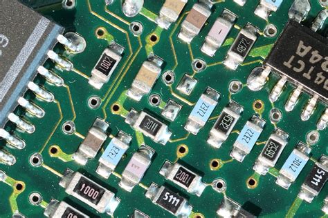
A detailed visual inspection checks for proper component placement, soldering, and overall PCB manufacturing quality. Magnifying lenses or microscopes are used to examine solder joints, trace widths, drill registration, and other small features.
Continuity Testing
Testing electrical continuity verifies the proper connectivity between PCB traces, pads, and vias. A multimeter set to continuity mode is used to check resistance and identify shorts or opens in the circuit. More advanced PCBs may require automated flying probe testers.
Functional Testing
Functional tests exercise the various subsystems and ICs to verify they perform as intended. The specific tests depend on the design but may include:
- Power up and power down sequences
- Analog and digital I/O
- Peripherals and interfaces like USB, Ethernet, SPI, I2C
- Displays, LEDs, and indicators
- Buttons, switches, and user controls
- Sensors and transducers
- RF and wireless functions
- Memory read/write
- Firmware programming and updates
- Stress tests like temperature or vibration cycling
Signal Integrity Analysis
For high-speed or RF PCBs, signal integrity (SI) analysis can help validate signal trace routing, impedance matching, crosstalk, and EMI performance. SI tests often require specialized equipment like oscilloscopes, spectrum analyzers, vector network analyzers (VNA), and near field scanners.
Compliance Testing
Depending on the end-application, the PCB prototype may need to undergo compliance testing to various safety and emissions standards such as:
- FCC Part 15 (unintentional radiators)
- IEC 61000-4-2 (electrostatic discharge immunity)
- IEC 60950-1 (IT equipment safety)
- MIL-STD-810 (environmental engineering)
- CISPR 32/EN 55032 (electromagnetic compatibility)
- UL 94 (flammability of plastic materials)
Catching compliance issues during the prototyping phase can avoid expensive redesigns and recertifications later. Some compliance tests can be performed in-house, but many require external test labs.

Benefits of PCB Prototyping
Effective PCB prototyping provides several key benefits:
Reduced Development Time and Cost
Identifying and fixing design issues early in the prototype phase is much faster and cheaper than making changes to a design already in production. Prototyping allows for rapid iterations to optimize the PCB before committing to volume manufacturing.
Improved Design Quality
The prototyping process provides opportunities to enhance the PCB design for better performance, reliability, and manufacturability. Rigorous testing and validation during prototyping leads to a more robust and higher quality end product.
Faster Time-to-Market
Streamlining the PCB development process with effective prototyping practices enables getting new products to market faster. Concurrent engineering techniques like rapid prototyping can further accelerate development cycles.
Increased Confidence
Thoroughly testing and validating PCB prototypes provides greater assurance in the design’s functionality and reliability. This increased confidence reduces the risk of potential failures or recalls after the product is released.
PCB Prototyping Best Practices
Here are some best practices to optimize the PCB prototyping process:
- Clearly define requirements and specifications upfront
- Leverage PCB design for manufacturing (DFM) techniques
- Use modular designs to facilitate debugging and future revisions
- Specify CAD designs in vector formats for precision manufacturing
- Choose PCB materials and components compatible with the fab house capabilities
- Consider panelizing multiple prototype iterations in the same manufacturing run
- Document the prototype fabrication and assembly process for traceability
- Establish standardized testing and validation procedures
- Use version control to track changes between prototype iterations
- Seek early feedback from stakeholders like manufacturing, marketing, and end-users
By adopting these best practices, development teams can streamline their PCB prototyping efforts to create better products faster and more efficiently.
Conclusion
PCB prototyping is a vital part of the electronics product development process. It enables designers to test and validate their concepts in the real world before investing in volume production. Effective PCB prototyping practices lead to faster development cycles, improved design quality, reduced costs, and greater confidence in the end product. As PCB technologies continue to push the boundaries of complexity and performance, efficient prototyping processes will be key to bringing innovative new products to market quickly and reliably.
Frequently Asked Questions (FAQ)
How much do PCB prototypes cost?
The cost of PCB prototypes depends on factors like the type of prototype, complexity of the design, material selection, and quantity. Rough estimates range from tens of dollars for simple perf boards to hundreds of dollars for multi-layer protoboards. Higher-complexity boards, exotic materials, and additional assembly can increase costs further.
How long does it take to get a PCB prototype?
PCB prototype turnaround times vary based on the specific design and manufacturer. Simple 2-layer protoboards can often be fabricated and shipped within 1-2 days, while high-density multi-layer boards may take 1-2 weeks. Adding component procurement and assembly can extend timelines. Expedited prototyping services are available at additional costs.
What are some common issues encountered in PCB prototyping?
Common issues in PCB prototyping include component footprint mismatches, incorrect hole sizes, signal integrity problems, power supply noise, insufficient heat dissipation, and poor solderability. Many of these issues can be avoided through careful design, DFM checks, and preliminary analysis before fabrication. Thorough testing and validation of prototypes is key to identifying and debugging issues.
What are some emerging trends in PCB prototyping?
Some notable trends in PCB prototyping include the increasing use of 3D printing for rapid enclosure development, wider adoption of high-density interconnect (HDI) technologies, growing demand for flexible and rigid-flex circuits, and more integrated sensors and modules for Internet of Things (IoT) applications. Cloud-based PCB design tools and turnkey prototype services are also gaining popularity, enabling easier collaboration and faster prototype delivery.
What should I look for in a PCB prototype manufacturing partner?
When evaluating PCB prototype manufacturing partners, consider factors like their technical capabilities, material selection, manufacturing tolerances, quality control processes, and design support services. Also look at their typical turnaround times, pricing, and order quantities to ensure they fit your project needs. Established certifications like ISO 9001, IPC Class 2 and 3, and UL registration are good indicators of quality. Recommendations from other designers and reviews of previous work can also inform your decision.


Leave a Reply